
Practical Optical Communication Systems
An intuitive approach.

Irrational Analysis is heavily invested in the semiconductor industry.
Positions will change over time and are regularly updated.
Opinions are authors own and do not represent past, present, and/or future employers.
All content published on this newsletter is based on public information and independent research conducted since 2011.
This newsletter is not financial advice, and readers should always do their own research before investing in any security.
Feel free to contact me via email at: irrational_analysis@proton.me
The quality and reach of a communication system is typically determined by the channel.
How wide is the channel? (bandwidth)
How flat is the channel?
Frequency selective fading.
Return loss (reflections).
ISI
Imagine you stumble upon a cursed monkey paw and wish for a channel that has 10’s of terahertz worth of spectrally flat channel bandwidth where insertion loss is measured in tenths of a dB per kilometer and reflections are almost non-existent.

The cursed monkey paw grants your wish, with hellish consequences.
Welcome to optical communication systems, where everything (except the channel) is a satanic nightmare and it’s a miracle any of this shit works at all.

For a detailed primer on communication systems, see this old post.

For an intro into co-packaged optics, see this old post.

For a brief primer on the current 1.6T tranceiver ecosystem, see this old post.

Today I will focus on the practical side of things. A lot of theory is going to get handwaved in the interest of time. Go read above old posts for theory.
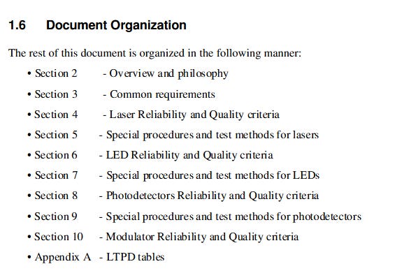
Contents:
Tuning
Electronics/Analog
Electronics/Digital
Photonics: Monkey Paw Says “Fuck You”
Periodicity and Filters
Modulation
The Driver Problem
The TIA Problem
Pointless Arguments and Modulator Tier List
Reliability
Standard Logic/Electronics Reliability: 1K Hour HTOL + ESD
GR-468: Another Hell From The Monkey Paw
Electronics Integration
GloFo “Fusion” Node
TSMC COUPE
Simulation, PDK, and Test Equipment Time Machine
Public Market Investment Corner
[1] Tuning
All complex systems need tuning mechanisms to optimize performance and yield.
Let’s compare electronics and photonics using some simple examples.
[1.a] Electronics/Analog
Here is an example of a tunable electrical amplifier inside a high-speed SerDes.
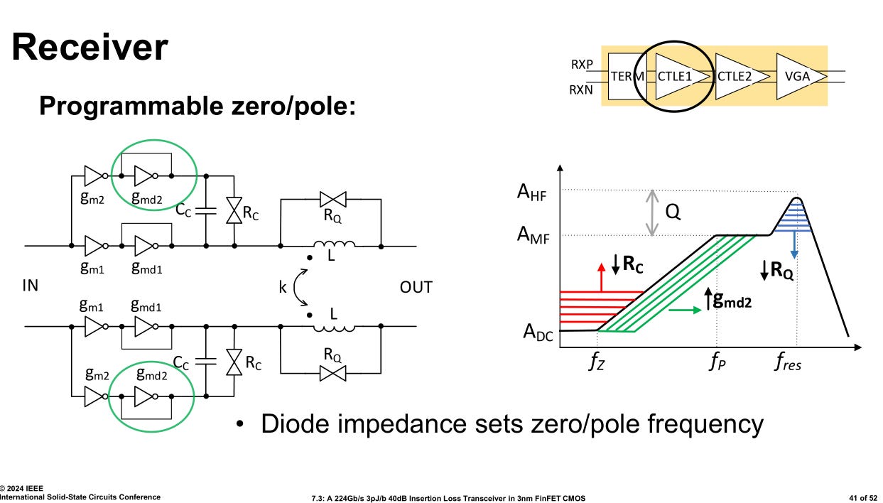
It is very important to have these tuning options because every electrical channel will be different. Two identical cables/connectors/PCB can easily have meaningfully different channel response and thus need different CTLE settings. This is a common thing.
Let’s take a more granular look at a generic analog circuit.
This simple amplifier consists of five transistors.
Four transistors (M_1-M_4) are the amplifier itself.
One transistor (M_b) is for tuning the gain aka bias adjust aka common mode adjust aka “how strong amplifier is”.
Real designs typically need MUCH MORE tuning circuitry. Here are some examples of tuning options I would like to have for this one circuit.
Granular (8-bit) Vdd adjustment.
At least 3 transistors to adjust bias instead of just one.
A varactor and potentiometer to adjust output impedance to match load.
Tunable decap for VDD.
Separate common mode adjustment for both NMOS and PMOS.
The nice thing about electronics is there are many options for adding such tuning circuitry. This means that yield can be high and performance can be tuned across many temperatures and channel/operating conditions.
[1.b] Electronics/Digital
Digital electronics are also highly tunable. Inside a modern chip, there can be thousands of sub-circuits with independently tunable clock-speeds.
Designers also include “chicken bits” that allow post-silicon validation to disable specific features.
Each sub-system in a digital logic IP block is highly configurable. This is a good thing.
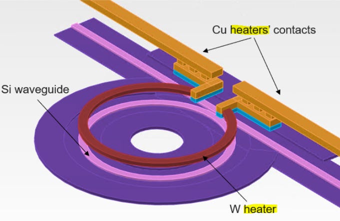
[1.c] Photonics: Monkey Paw Says “Fuck You”
All photonic structures are tuned with tiny heaters.
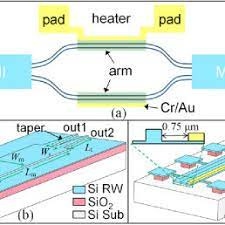
Those of you with electronics background understand how fucked up this is.
For everyone else, let me express how painful this is in the form of gif.

Almost zero granularity or programmability. Struggling to find words to express how obnoxious this tuning issue in photonics is.
Quick detour is necessary.
https://en.wikipedia.org/wiki/Proportional%E2%80%93integral%E2%80%93derivative_controller
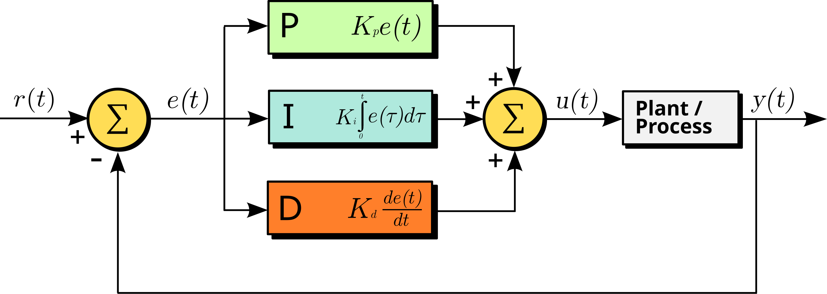
Within engineering, there is a field called control theory.
A very popular (fundamental) control loop is called PID.
The system has a feedback mechanism to measure error.
Then the error, integral of the error, and derivative of the error are computed with a scaling factor for each.
Closed-loop PID control of parameters is a useful tool.
Directionally, electronic systems have maybe 5-10% of parameters under closed-loop PID control.
In photonics, almost everything is PID controlled.
THIS IS NOT A GOOD THING.
THIS IS FUCKING PAINFUL.
Each PID control loop needs precise tuning of the coefficients. Debugging one of these things is very painful.
Within electronics, people often find that hardcoding values and disabling a PID controller leads to better results. In photonics, you can’t disable the PID loops because those fucking tiny heaters are unstable.
(this applies to all photonic structures… even MZIs in many situations need PID control)
The best part is, all the structures on a photonic chip dump thermal noise into each other. Adjusting the PID control of one structure regularly fucks up control of other structures. Standard debugging tactics like “lets turn off parts of the chip to isolate issue” don’t work.
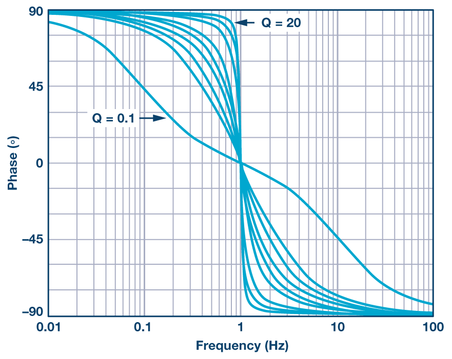
[2] Periodicity and Filters
Filters are an important tool for building communication systems.
Need a way to get rid of unwanted junk.
Here are some examples of filters found within traditional electronic systems.
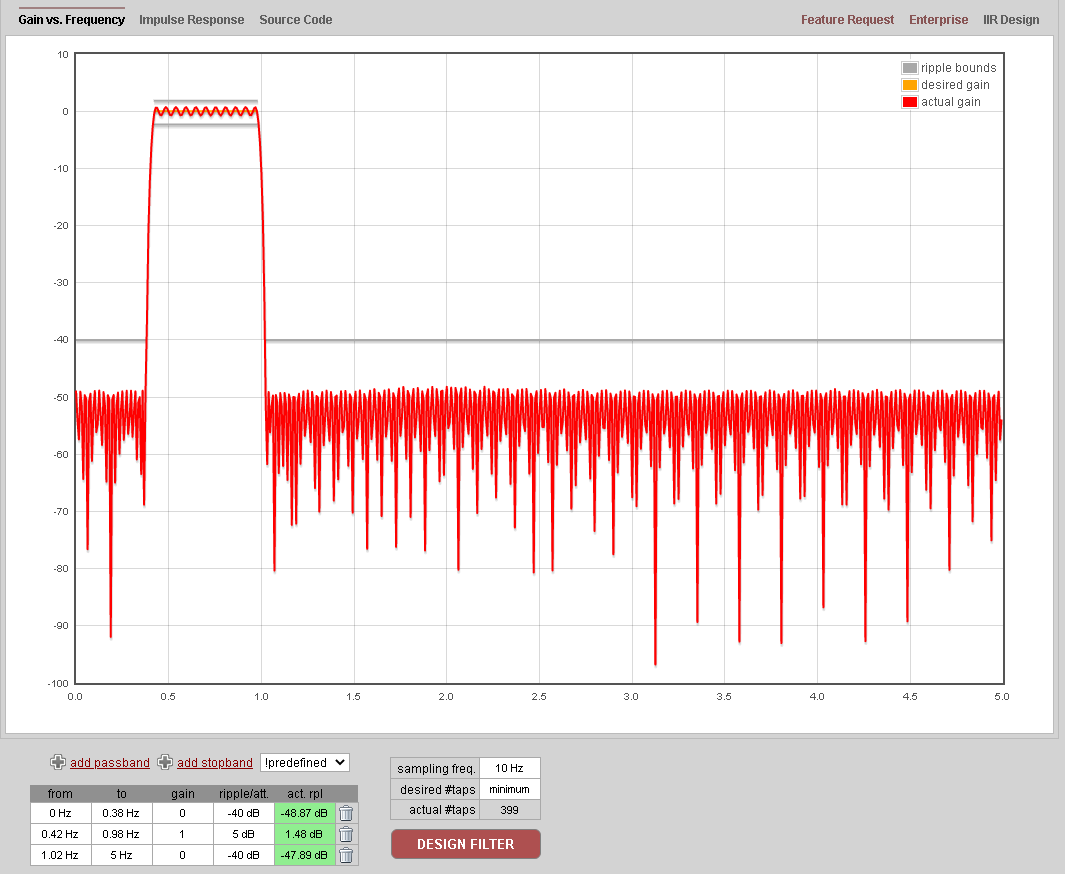
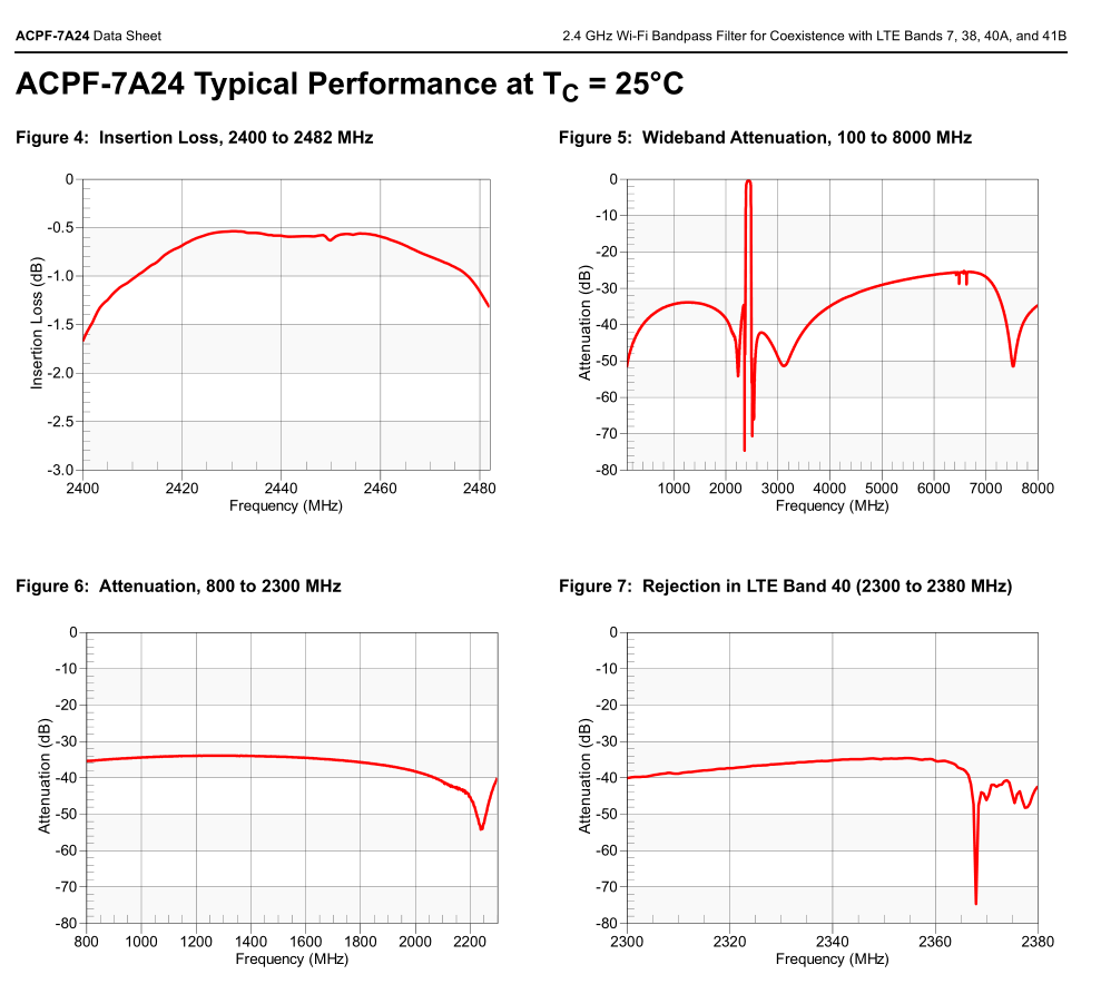
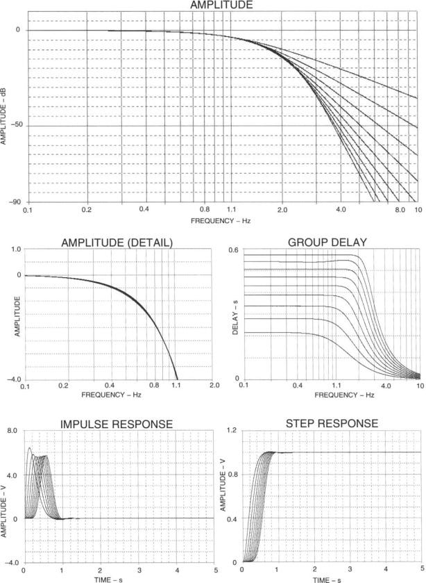
All of these analog and digital filters (within electronics world) have similar attributes:
Flat in the passband (good)
Sharp rejection of stopband (good)
Minimal weird spikes in the stopband (good)
Spikes in stopband still have over 30 dB rejection.
Not periodic.
Can design filter so spike is in less-problematic part of stopband.
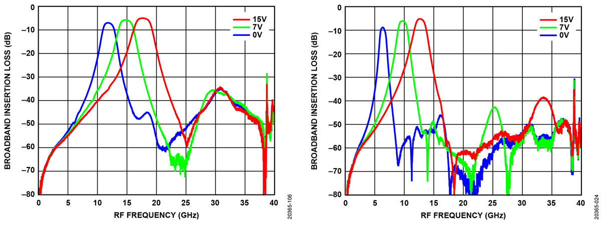
Photonic filters are the opposite. (complete dogshit… hilariously bad)
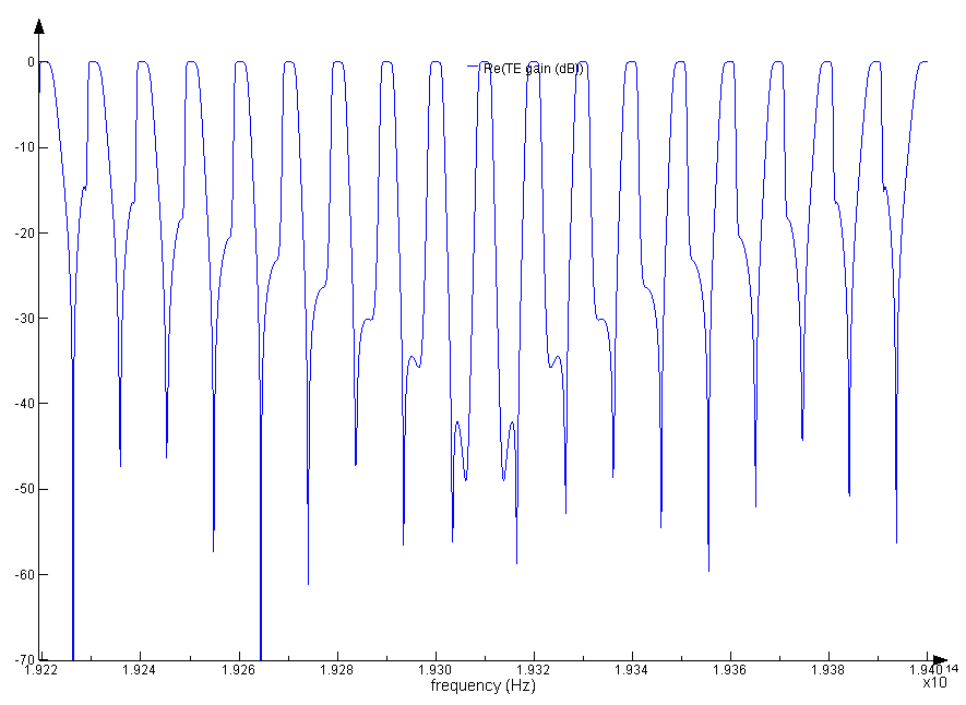
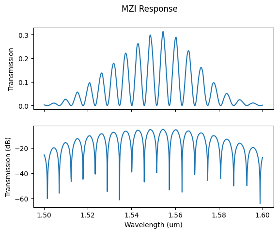
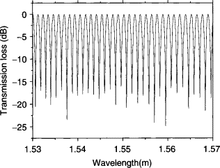
Not only are the filter responses dogshit (trash insertion loss, trash rejection ratio, trash passband flatness), they are also fucking periodic.
This is mind-blowingly annoying.
NOTHING IN ELECTRONICS IS PERFECTLY PERIODIC LIKE THIS PHOTONICS SHIT.
[3] Modulation
Modulation (in this context) is the process of making an electrical signal wiggle light.
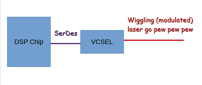
[3.a] The Driver Problem
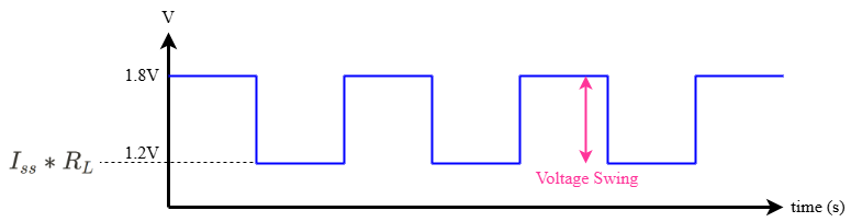
In general, optical modulators require high voltage swing (2+ Volt) and are usually singled-ended, commonly denoted by Vpp which stands for voltage-peak-peak.
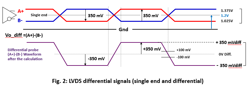
All high-speed electrical SerDes are differential. Ignore this for now. Go read old posts if you want to understand why differential signaling exists.
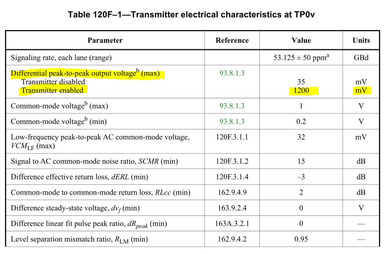
Anyway, as an example, Ethernet SerDes is limited to 1200 mV Vpp.
High-speed SerDes has swing of around 400-1100 mV and is optimized for 600-800 mV operation.
Die-to-die SerDes (UCIe, NVLink D2D, Broadcom MAX, Marvell D2D, Elyian) operate around 400 mV with an absolute theoretical maximum in the 800 mV ballpark.
So if you try the drive an optical modulator with an Ethernet SerDes directly, your system wont work at all.
Certain companies like to argue about how their modulators require lower voltage swing but fundamentally, all optical modulators need an external driver (amplifier/booster) to function.
(all optical modulators suck)
Having an external driver in your system is not a good thing. It is a necessary evil.
More noise.
More power and cost.
Packaging/integration challenges.
Interoperability issues.
This is one of the reasons why LPO transceivers have taken so long to finally ramp.
[3.b] The TIA Problem
Once light makes it to the receiver of an optical communication system, it needs to be converted back into electricity using a photodiode (PD).
You know bout LEDs right? You looking at LEDs right now reading this.
LED convert electricity into light.
PD does the opposite. Simple.
The problem with PDs is the efficiency is… shit.
Electrical signal coming out of the PD is super weak and needs to be amplified with a transimpedance amplifier (TIA).
TIA is **not** an optics-specific component.
There are two basic amplifiers.
One is called TIA.
The other is called Gm.
You can chain these building blocks to create more complex amplifiers.
You can put TIAs on the SerDes chip too. This is a common strategy. Problem is, you need a VERY POWRFULL TIA to boost the shitty signal coming out of PDs.
Very Powerful means…
Poor power efficiency.
Adds lots of noise.
Expensive.
Packaging/integration challenges.
Having a discrete TIA in your system is not a good thing. It is another necessary evil.
[3.c] Pointless Arguments and Modulator Tier List
The photonics industry is full of people making the following argument:
“My modulation tech is better than yours. Your modulation tech will never work.”
Within traditional transceivers, there are four options.
VCSEL
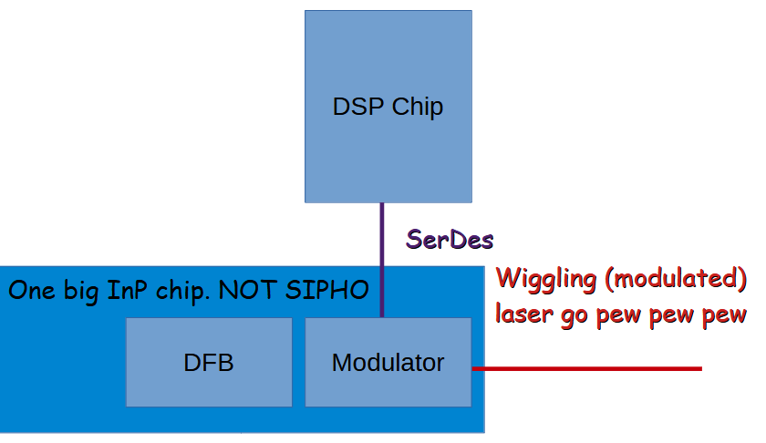
EML (InP monolithic EAM)
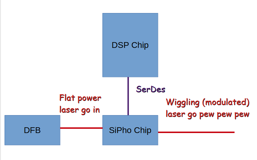
SiPho MZI
SiPho DR (single wavelength) Ring
My old post on this assumed CWDM 4 wavelength.
Old post wrong. It’s single-wavelength DR rings.
Conclusions still same.
I don’t edit old posts. Public record of mistakes and wrong calls is good thing.
Option #1 does not work for 200G per lane (1.6T transceiver) modulation. Reliability bad. Certain companies are coping that they gona get 200G VSCEL to work.
Nvidia is using option #4 for their 1.6T transceivers. They save power because the optical insertion loss of ring modulators is much lower than MZI or EAM.
But frankly, there is no reason to argue on option #2 vs #3 vs #4.
This is a business, not a philosophical debate.
Ship as many units as possible at the highest gross margin as possible using whichever of the three viable options you want. There are tradeoffs. That’s the point of engineering.
For co-packaged optics, there are different options.
VCSEL
SiPho DR MZI
SiPho DR (single-wavelength) ring
SiPho CWDM (4 wavelength) ring bus
SiPho DWDM (8+ wavelength) ring bus
SiPho (Germanium) EAM
Micro-LED
Let’s set aside #7 for now.
(will shit on micro-LED later)
Honestly, all options 1-6 are theoretically viable.
I find it very irritating when people shill their modulator technology and make questionable arguments.
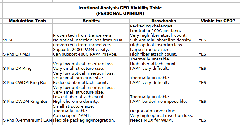
Here is my personal opinion in tier form.
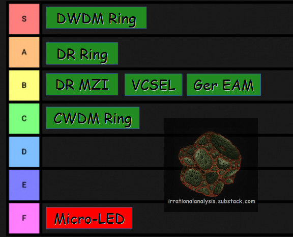
In 2026, Nvidia is going to ship at least 10K units of CPO switches using DR rings running at 200G PAM4. (number is much higher…)
*Note: There is a reason why Nvidia is not using WDM in their initial CPO product. Many rings packed closely together lead to MASSIVE thermal crosstalk issues. Nvidia has not solved DWDM ring bus stability yet and they are the clear leaders. Something to think about.
THERMAL STABILITY WITH ONE TRING ACTIVE != THERMAL STABILITY WITH ALL RINGS ACTIVE AND DUMPING NOISE INTO EACH OTHER
THERMAL STABILITY WITH SLOW TEMPERATURE RAMP (DEGREES C PER SEC) DOES NOT PROVIDE USEFUL INFORMATION OR PROOF OF STABILITY.
Also in 2026, Broadcom is going to ship at least 10K units of Tomahawk 6 CPO switches using 200G PAM4 modulated MZI. (number is much higher…)
I feel like a reasonable definition of success for a CPO system is to meet all of the following requirements:
Ship at least 10K units in one year.
Achieve gross margins of at least 20%.
If your margins suck, that means yield and thus technology suck.
Are you a business or a science project?
If your margins are worse than Chinese transceivers then you might have a problem.
Pass GR-468, a reliability pre-requisite for people to buy your product.
More on this in next section.
As far as I can tell, Nvidia and Broadcom are the only two companies who will meet these success requirements in 2026.
What if Nvidia and Broadcom wipe everyone else out? It’s a real possibility lol.
Now let’s talk about micro-LED.
In order to reduce the chance of a new cease-and-desist letter getting added to my collection, I will limit discussion to a specific paper published by Microsoft.
Do not extrapolate my commentary on the Micro[soft] LED paper with any other company that might work on something similar.
https://www.microsoft.com/en-us/research/wp-content/uploads/2025/08/benyahya25mosaic.pdf
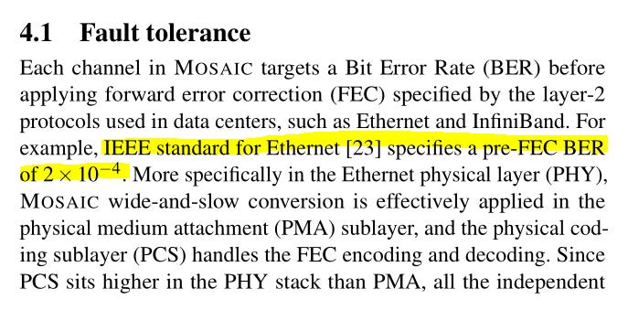
I happen to have a pirated copy of IEEE 8021.3ck-2022. Also happen to be very familiar with this specification.
The citation in this Microsoft paper that pre-FEC BER needs to be 2e-4 or lower is technically correct.
Within industry, this 2e-4 spec has been widely ridiculed for years. Its complete bullshit.
Real systems need at least 1e-7 pre-FEC BER MINIMUM TO BARELY PASS FEC TESTING.
A target of 1e-9 under adversarial conditions (HTHV+PSRR+JTOL+ITOL+PPM) is what people actually want. Clean operating conditions should hit 1e-11 or lower.
Every hyperscaler went to IEEE/Ethernet committee and complained that this 2e-4 spec is bullshit.
This is why 200G standard (IEEE 802.3dj) made all compliance testing require **post-FEC data at 2e-13**.
2e-4 pre-FEC BER target is bullshit. Everyone in industry knows this. ****Ethernet changed spec to 2e-13 post-FEC for a reason!****
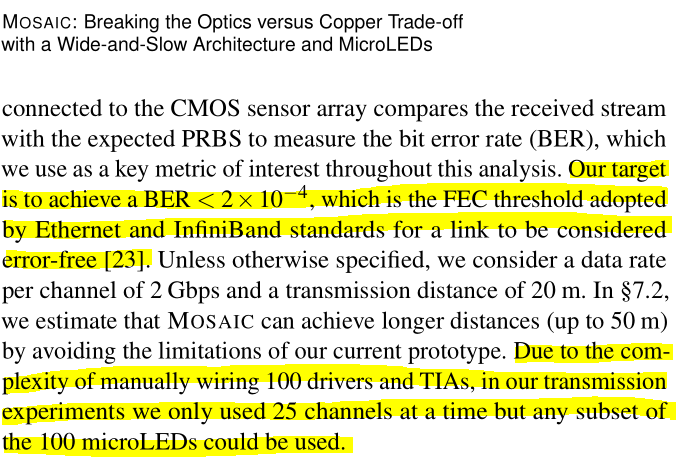
Showing data with only 25/100 channels is a huge red flag. Micro-LED solutions encounter massive electrical crosstalk issues. Turning off 75% of the channels massively distorts performance into an unreasonably favorable state.
1e-7 is frankly a generous threshold. I am being nice. Should draw the line at 1e-9.
The amount of power and digital area that needs to be allocated to FEC just to get this cheezed low-crosstalk (only 25/100 channels active) demo is truly hilarious.
There is no indication at what temperature these (bad) BER numbers were measured at. Another huge red flag.
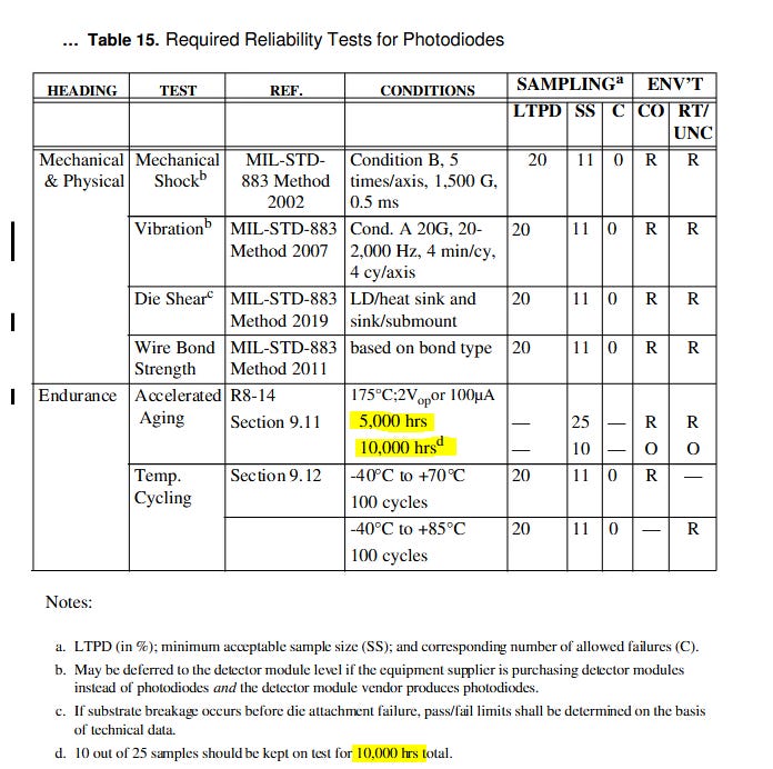
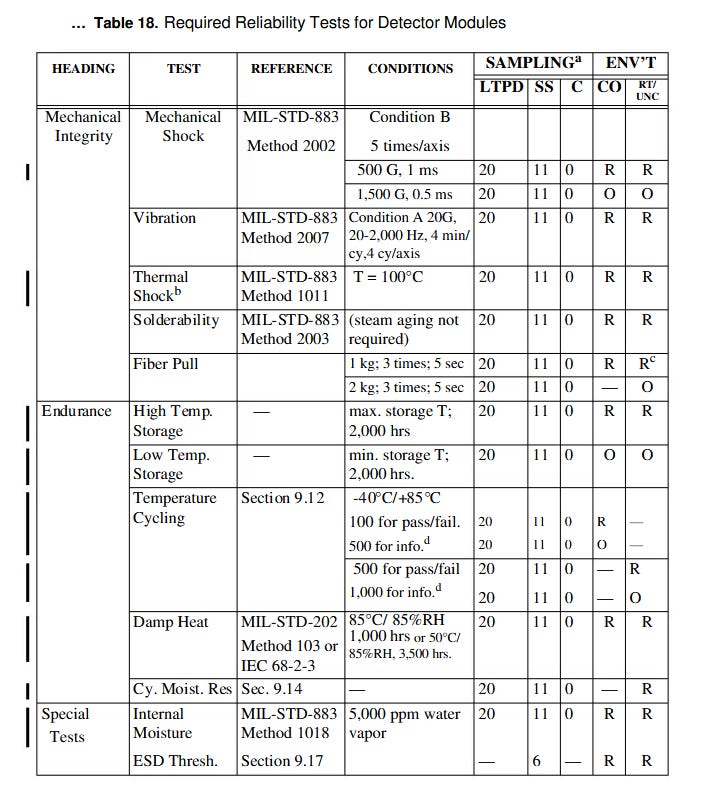
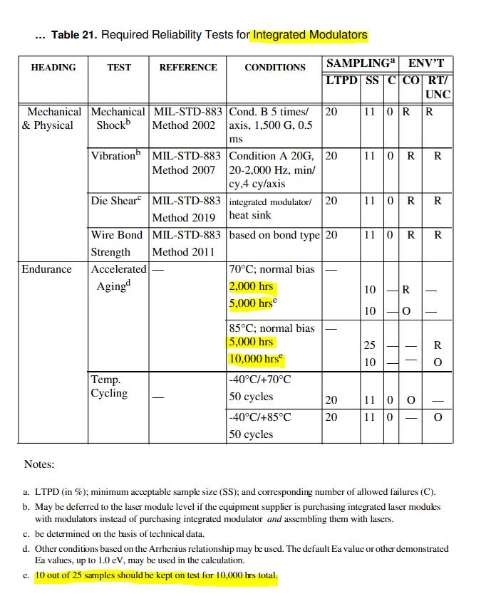
[4] Reliability
I briefly touched on optical reliability in my recent OCP 2025

Some more details here. I think it is helpful to compare electronics and photonics again.
[4.a] Standard Logic/Electronics Reliability: 1K Hour HTOL + ESD
Reliability of logic chips (electronics) is generally simple.
Here is the whole process with some typical numbers:
Measure performance of a set of devices (typically 80-160 packaged dice) at room temperature and nominal voltage.
Place all devices into an oven.
Set the devices to run at +20% above nominal voltage on all power rails.
Configure the oven temperature such that all device internal temperature monitor diodes read 125C or higher.
Run all devices continuously for 48 hours, monitoring performance and current draw on all power rails.
Remove devices from oven, measure at room temp, nominal voltage.
Repeat steps 2-6 again at 168, 500, and 1000 hours.
This test is called “high-temperature operating life”, AKA HTOL.
https://en.wikipedia.org/wiki/High-temperature_operating_life
Broadly, the goal is to check a design for electromigration issues.
HTOL takes 1000 hours, which translates to about 43 days theoretically.
In practice, shit goes wrong. It takes more like 3 months realistically.
Modern EDA software (Synopsys, Cadence, Ansys) is generally quite good at simulating electromigration, commonly referred to as “EM” by designers.
If a design fails HTOL, someone fucked up and is probably going to get fired.
If a design passes HTOL, it is theoretically reliable up to 10 years of nominal operation. The numbers change on a case by case basis. For example, a particular chip might need to HTOL at (135C, +25% voltage) instead of (125C +20% voltage) to meet this industry-standard 10 year reliability criteria. I am just giving the common numbers.
The next major category to reliability testing for electronics is ESD, electro-static discharge.
Procedure for this is very simple.
Measure the performance of a lot of devices (10-20 packaged dice) at NTNV.
Use a special machine to “zap” certain bumps of each device at increasingly higher voltage.
Not all bumps need to be checked for ESD.
Only bumps sensitive to ESD such as high-speed signal, IO, or memory.
VDD and ground bumps generally safe in most cases.
Measure the peak current of each zap.
Measure the performance of each device after zap.
Use a scatterplot to find where the design failed. (max tolerable current)
Above link is a good resource for more details. I plan on writing about reliability testing in more detail next year. For now… backlog of more interesting topics.
Broadly speaking, HTOL and ESD are the main reliability gates for electronics. Of course, automotive and military-grade parts need more reliability testing. But… the standard reliability testing is not that bad.
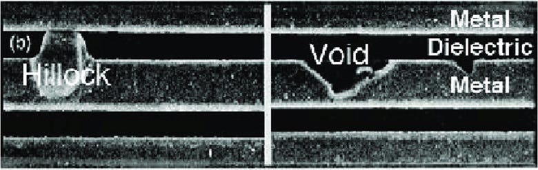
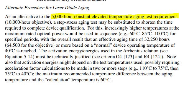
[4.b] GR-468: Another Hell From The Monkey Paw
It’s so much worse. Legit order of magnitude more painful.
Investors, say the “GR-468” keyword to anyone who claims their optical product is ready for mass production. They either gona shit themselves or show you the data.
GR-468 is a hard requirement set by all major customers. This is not some “legacy” spec that can be ignored or handwaved. It is a satanic nightmare that must get done.
No GR-468 == you die

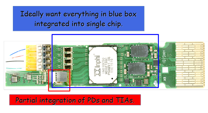
[5] Electronics Integration
One of the major challenges that has plagued optics-land for decades is integrating the electronics.
Ideally, you would want all of those drivers, TIAs, and photonics integrated into a single chip. Lower cost, better power efficiency, lower noise, higher performance.
The normal approach is to just have flip-chip packaging for the PIC, EIC, and (if applicable) discrete components.
Here are the two novel approaches.
[5.a] GloFo “Fusion” Node
Global Foundries GFS 0.00%↑ has a special process node that I like to call the “Fusion” node.
Their public marketing is unfortunately confusing.
https://gf.com/technology-platforms/silicon-photonics/
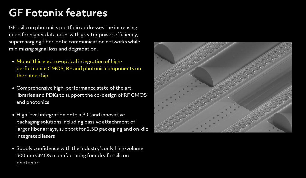
They use the “Photonix” branding for completely different process nodes.
Set aside the photonics-only nodes. Nothing I am about to write pertains to those nodes.
When GloFo talks about ”monolithic electo-optical” or “integrated photonics + RF CMOS” they are talking about what I call “the Fusion node”.
GloFo Fusion node is unique within industry. I am not aware of anyone else who has tried this.
They basically take a photonic process node and an 45nm-class electronic process node and smash them together.
This means that the “Fusion” node has a crazy layer count. When I first heard about how many layers this thing has and the cycle time, I burst out laughing.
Cycle time is worse than 3nm logic. It’s hilarious.
Now you have to understand that I talk to many people across dayjobs and though this hobby. On every topic, there is always a distribution of opinion.
Except on GloFo Fusion node.
I have had conversations with 40+ engineers across 7+ companies and the GloFo Fusion node is universally derided. Not one person had a nice thing to say about GloFo fusion.
Some common themes….
45nm-class electronics not good enough for most applications, especially CPO.
45nm-class GloFo electronics much worse than TSMC N45.
Massive electrical crosstalk issues.
Massive thermal crosstalk issues.
Reliability concerns due to warpage from having so many layers in the process.
Painful cycle time which delays R&D efforts.
Way too expensive.
Poor yield.
Optics industry went through a phase where this GloFo Fusion node was viewed as the “least-worst” option.
Until TSMC released COUPE.
[5.b] TSMC COUPE
COUPE is TSMC’s answer to the “electronics integration” problem.
It’s amazing. Go read old posts for detailed coverage on why.
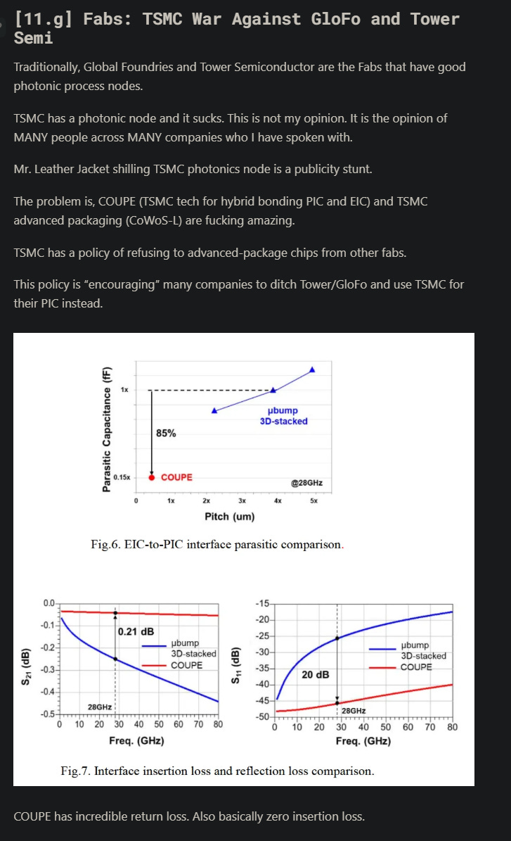
Problem is cost. Hybrid bonding makes this solution very expensive.
TSMC has marketed COUPE for both traditional transceivers and CPO.
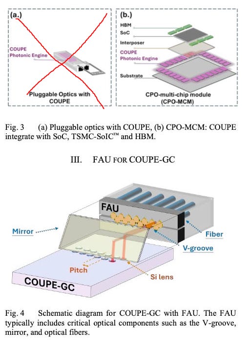
Need to put my foot down here and say COUPE will NEVER BE VIABLE FOR TRANCEIVERS. Too expensive and frankly overkill.
[6] Simulation, PDK, and Test Equipment Time Machine
All of this is so much worse than electronics. Feels like going back 15-20 years. Remarkable the optics/photonics industry has functioned all of this time with such crap tooling.
[7] Public Market Investment Corner
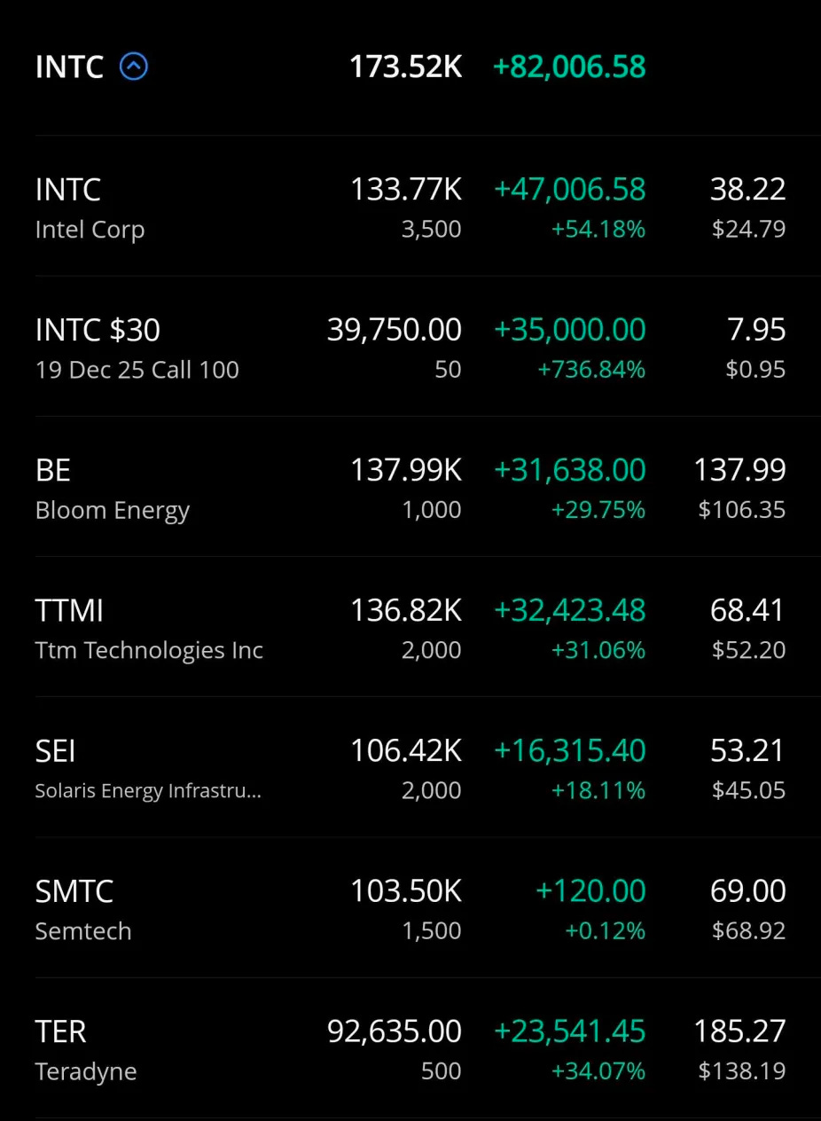
Too lazy to update my long-only account manual spreadsheet. Sold all my Verizon, bought more Keysight with the proceeds. Goto old posts to find long-only holdings.
Here is trading account.
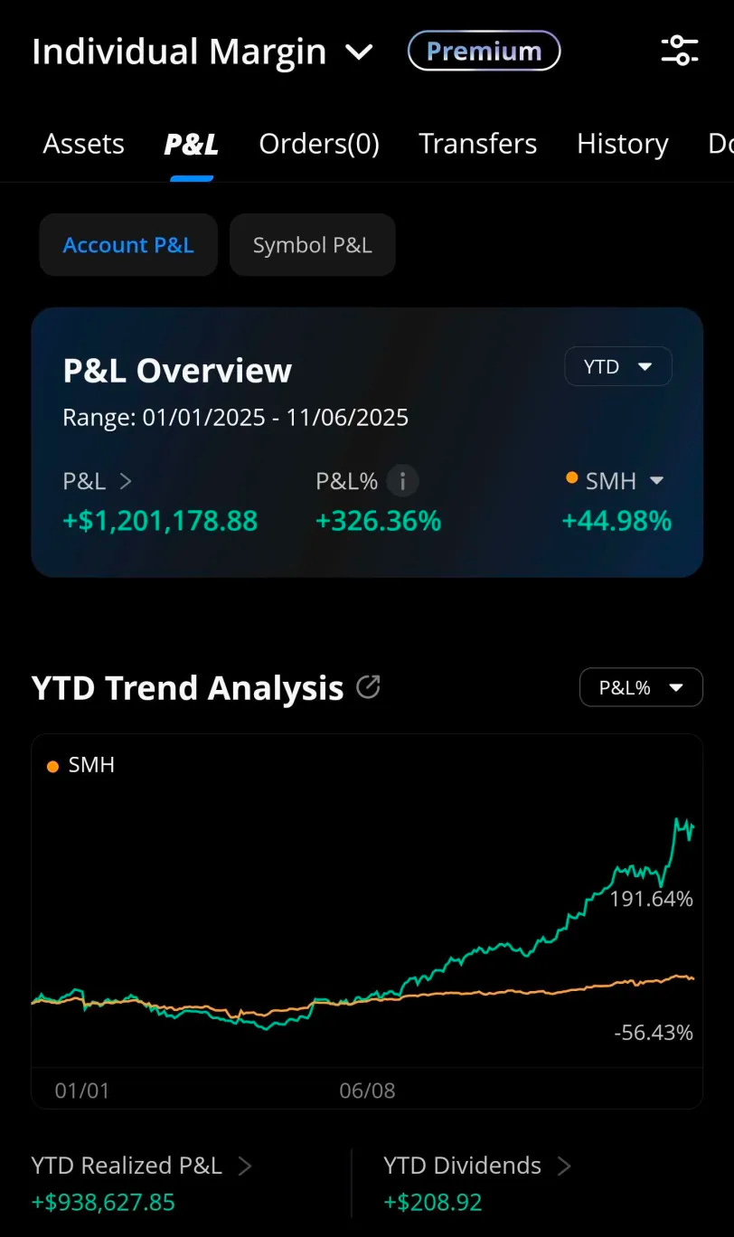

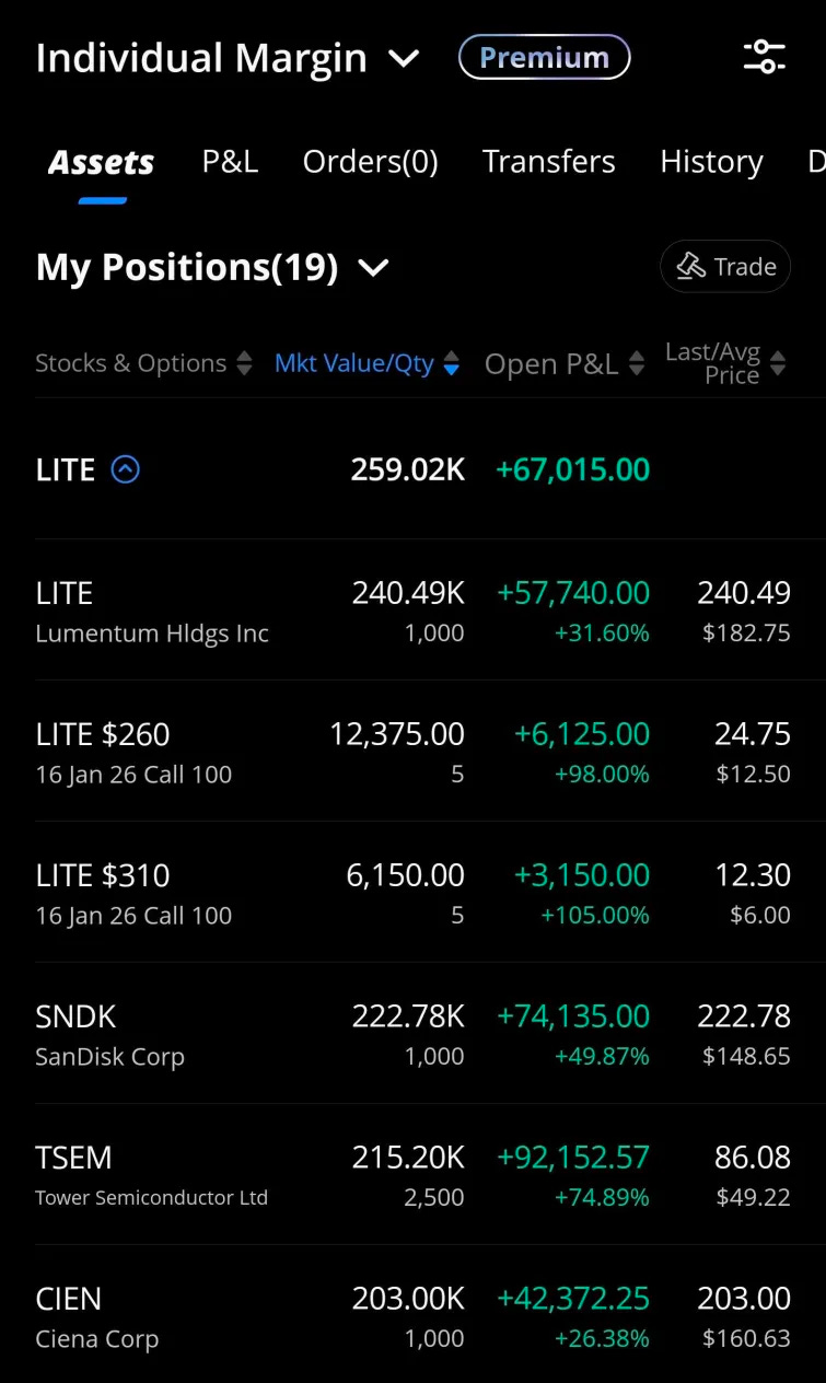
Note: My average price for LITE 0.00%↑ shares was $154 but I paper handed and sold half the position before buying back in after-hours while listening to the call.
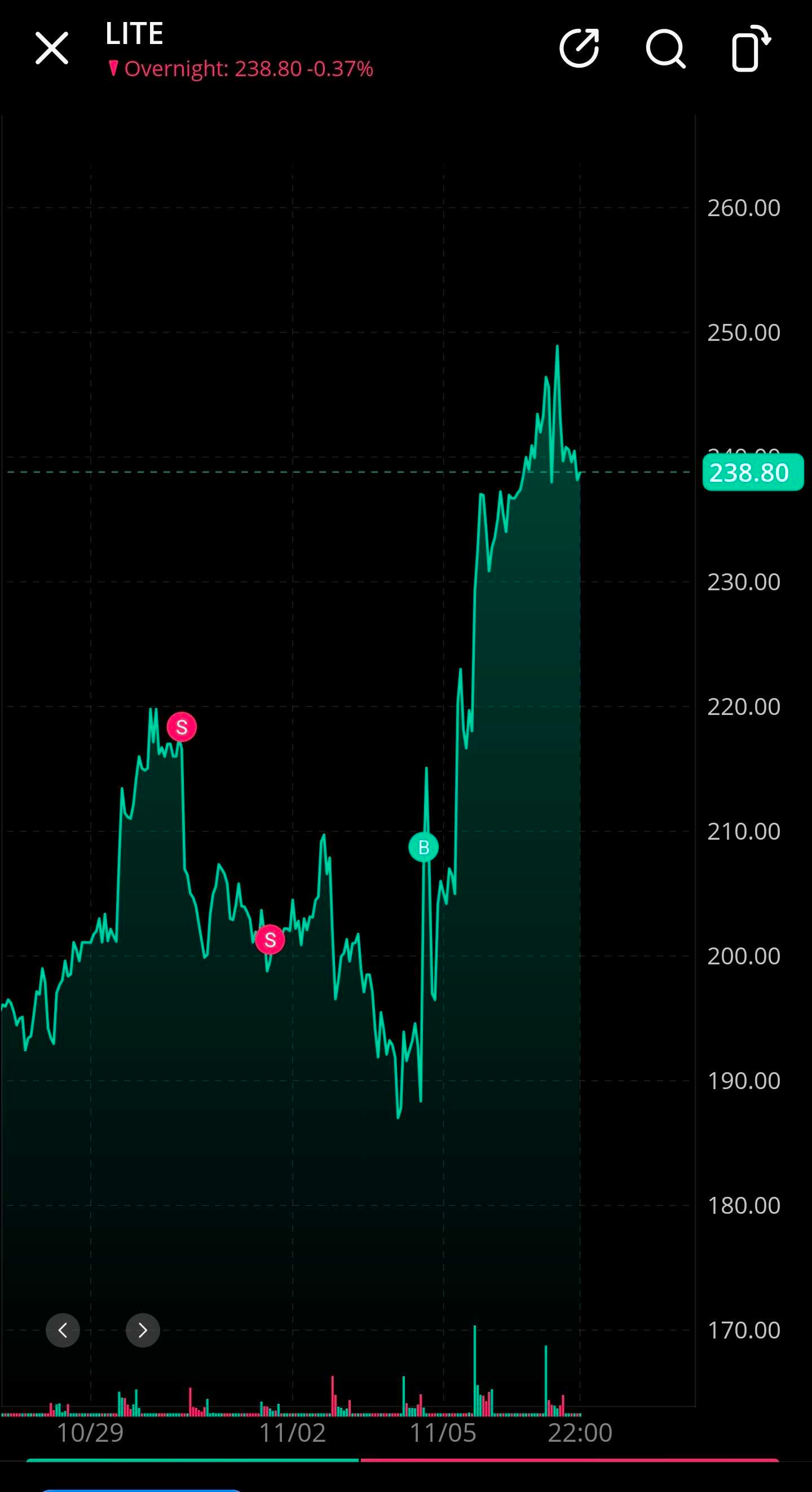
Ends up not mattering in terms of non-tax performance but it makes my taxes this year suck slightly more. I still need to pre-pay like $250K in taxes before EOY lol.
Anyway, here is brief opinion of several names in table form. Some earnings call analysis afterwards.
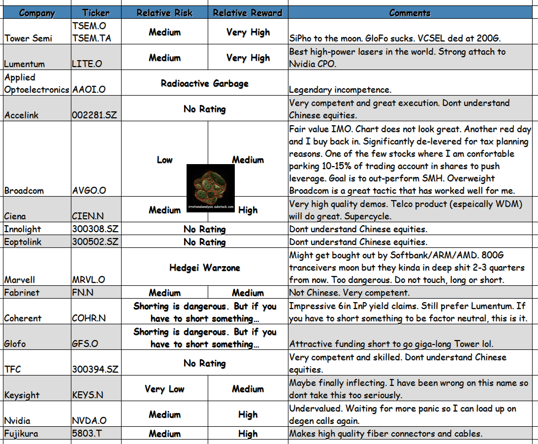
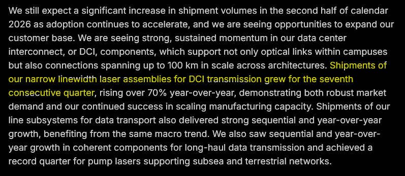
Lumentum and Coherent earnings calls were super interesting.
Let’s start with Lumentum.
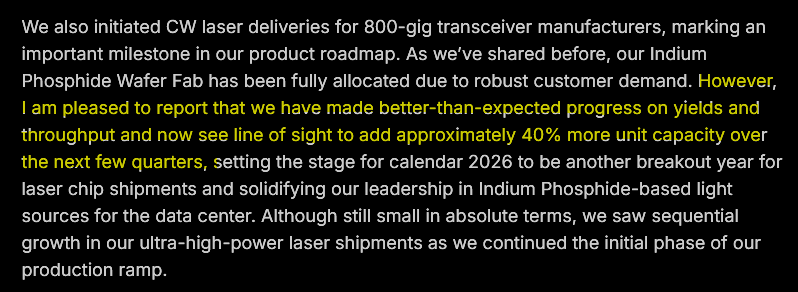
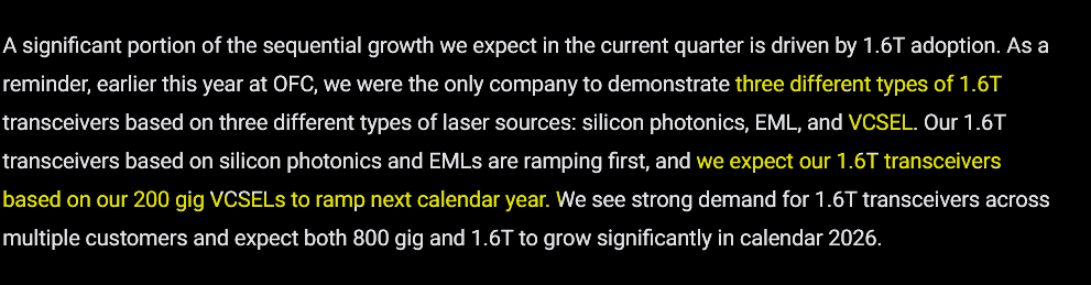
They were sold out, added 40% more capacity by migrating for 3in to 4in InP wafers, and are sold out again lol. Hyper-omega bullish.
I like the Lumentum CEO. He seems to actually know what he is talking about.
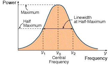
Linewidth of a laser is typically defined as the frequency span of the 3dB cutoff.
1 MHz is considered to be good linewidth. For long-reach telecom applications, you want much more narrow.
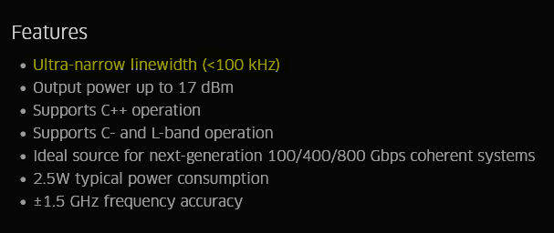
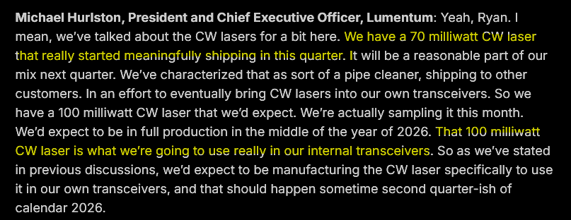
CW lasers have traditionally been 20-40 mW.
70 mW is a nice jump and they are ramping to 100 mW. Very nice.
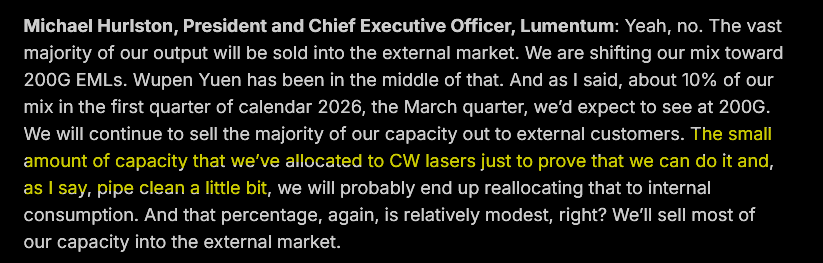
Pipe-cleaning for Nvidia CPO ramp H2 2026.
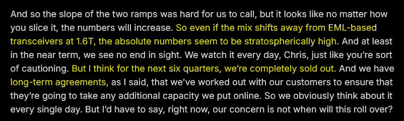
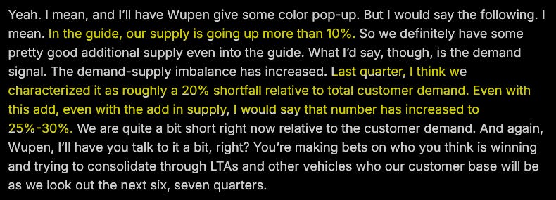
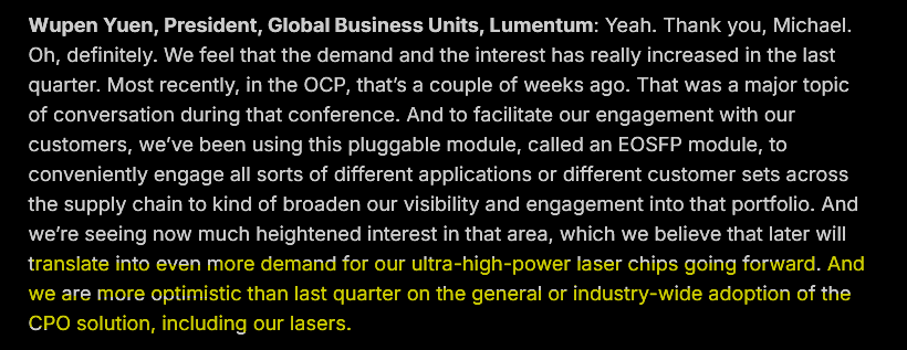
ultra-high power laser = 250-350 mW class
Nvidia CPO ramp is bigger now.
Lumentum also appears to hint that they are talking to Broadcom for CPO ELSFP which is uh… surprising.
Coherent call now.
VCSEL is not going to work at 200G per lane. Reliability issues. I don’t understand why Coherent keeps coping and bringing this up.
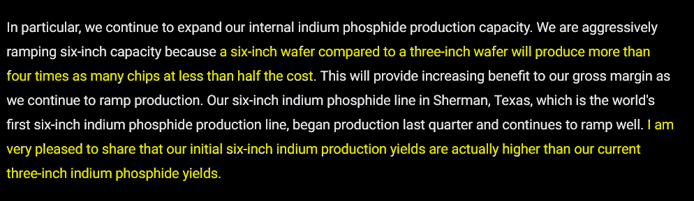
This claim that 6in InP yields are higher than 3in is frankly shocking. I am not sure how this is possible. Like its legit unbelievable.
Yield is usually defined as a percentage of good dice.
Maybe Coherent CEO is cheezing this by re-defining yield as number of dice at ISO cost.
There is also the question of how they define yield in terms of quality.
If yield is “sellable EML” and only a small number of EML can work at 200G speeds while vast majority only work at 100G speeds, that would be good to know lol.
Coherent buys a lot of EML from Lumentum. There is a reason for this. (quality…)
Bro if your 6in yield is so amazing and you doubling capacity why u buying **MORE** EML from Lumentum lol.
Coherent is around 2-years behind on ultra-high-power CW lasers.
Lumentum is clear leader.
Finance friends, go ask Coherent CEO how far they are with GR-468 of these 400 mW lasers. Then go ask Lumentum CEO the same question.
My email is public at the top of every post. Send me what they say plz.
Coherent OCS tech has massive optical insertion loss. It’s like 3 dB lol.
Liquid-crystal OCS is indeed way better reliability than MEMS OCS.
But what the hell u talking about with superior performance? Bro I have seen the insertion loss of public demo. It’s not good.
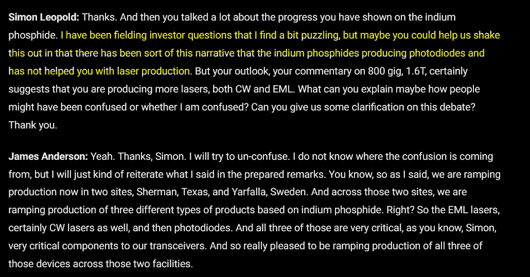
Well… manufacturing PD is much easier than manufacturing lasers.
Sounds like some of the finance-crowd have picked up on something and there is trash talk behind the scenes.
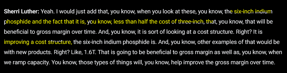
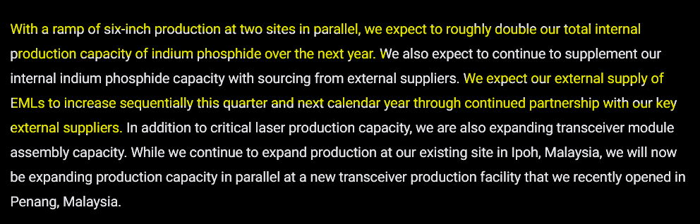
If cost is half then what is gross margin improvement?
Cost + Yield —> Gross Margin
The more Coherent execs talk about 6in InP amazing yield the more suspicious I get.
Messa smell bullshit.
VCSEL IS NOT RELIABLE AT 200G PER LANE. SHOW GR-468 DATA. BROADCOM IS WORLD-LEADER IN VCSEL AND THEY STOPPED AT 100G/lane.
higher yields could also be due to newer tools relative to 3inch
For COHR, maybe 6in has higher yields than 3in due to focusing more engineers resources there and essentially abandoning the yield improvements of 3in?