
A Background-Proof Guide on Co-Packaged Optics
The future of high-speed datacenter communications.

Irrational Analysis is heavily invested in the semiconductor industry.
Please check the ‘about’ page for a list of active positions.
Positions will change over time and are regularly updated.
Opinions are authors own and do not represent past, present, and/or future employers.
All content published on this newsletter is based on public information and independent research conducted since 2011.
This newsletter is not financial advice, and readers should always do their own research before investing in any security.
Feel free to contact me via email at: irrational_analysis@proton.me
Welcome to a deep-dive on co-packaged optics.
Your background is irrelevant. Everyone will be able to learn something new, even the pod monkeys.

Some basic communication systems concepts will be hand-waived in the interest of time. I want to focus on optics specifically with this post.
Read this old one if you are interested.
The material for this post was developed from three primary sources:
Incredible Texas A&M Professor Sam Palermo: https://people.engr.tamu.edu/spalermo/ecen721.html
Broadband Circuits for Optical Fiber Communication 1st Edition
Back in college, I was poor and usually pirated books.
Now, I regularly achieve losses of $20K or more in one day in one account. 🤡🤡🤡🤡🤡
Makes it much easier to treat myself to expensive $100-$300 new copies of textbooks. 🤡
A variety of public research papers I found while browsing Google Scholar.

There will be a section at the end discussing public companies who have either developed CPO solutions or are involved in the supply-chain.

Sidenote: I listen to a single electronic music track for hours on end while writing these long posts. Track changes every few weeks.
Open this up on a new tab, right click, and enable looping on YouTube for the full experience.

Let’s get started.
Contents:
The Channel Problem
Electrical Channel Examples
Optical Channels are Amazing
Narrowband Carrier Waves: An Intuitive Approach
Linearity and Differential Signaling
Light Sources (Lazer go pew pew pew)
Photodetectors
Modulators
Direct Modulation (laser input current wiggles)
External Modulation (constant laser output is wiggled later)
Electroabsorption
Mach-Zehnder (MZM)
Micro-Ring Resonators (MRM)
Two Tribes and a False Choice
Electrical Periphery: TIA and all that
Incorrect Obsession with Silicon “Beachfront/Shoreline”
Photonic Process Nodes
Walkthrough: Nvidia Quantum-X GTC 2025 Announcement
Walkthrough: Broadcom Hot Chips 2024 Baily Presentation
Public Market Investment Corner
Transceiver Exposed Companies are Fucked
oDSP Exposed Companies also Fucked (COUGH COUGH MARVELL)
CPO Developers: Nvidia, Broadcom, and Marvell
Laser Manufacturers: Lumentum and Coherent
Outsourced Assembly: Fabrinet (is better than everyone else)
Glass: Corning and Nittobo
Fabs: TSMC War Against GloFo and Tower Semi
[1] The Channel Problem
Every communication system has a channel that sits between the transmitter and the receiver.

It could be air, copper, optical fiber, or a string between two tin cans.

Math abstracts the attributes of a communication channel. The most important of which is frequency-selective fading.

If you take a narrow enough slice of bandwidth, the channel response is “flat”, simply weakening the signal in a uniform manner.
Communication systems are designed around the channel.
For example, wireless channels are nasty so all modern standards (4G/5G, WiFi) use OFDM.

The channel (typically 20-100 MHz wide) is divided up into 12 KHz sub-segments.
[1.a] Electrical Channel Examples
This is what a real, rather favorable electrical channel looks like.

There is some loss (dB) at the Nyquist frequency which represents how “weak the signal becomes” as it passes through the channel.
But what many people miss is the frequency quality of the channel. As frequency goes up, the ripples and junk become much worse. This places enormous stress on the receiver, blowing up digital signal processing complexity, area, and power.
Here is another example:

The blue channel consists of two very short, high-quality coax cables and a small PCB made of very high quality prepreg and core dielectric material.
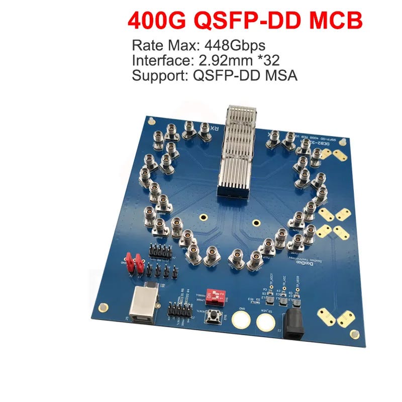
The red channel is something more realistic. A regular, commercial QSFP-DD passive copper cable is added to the path alongside a SMA breakout board.
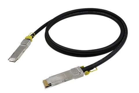
As you can see, the red channel looks horrible. This is the fundamental problem with electrical high-speed links going forward.
Magic materials do not exist. 448G electrical SerDes is not going to work in any reasonable manner.

Co-packaged optics is the future.
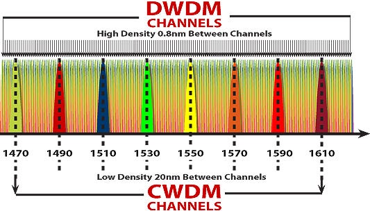
[1.b] Optical Channels are Amazing


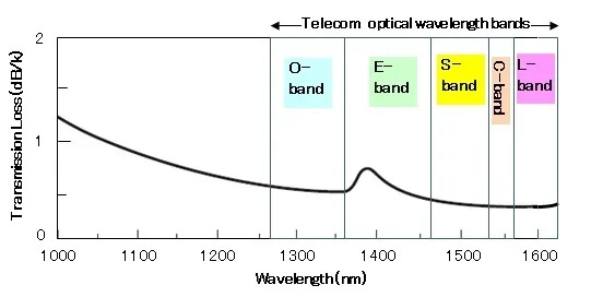
Note that the x-axis is in nanometer. Converting to Hz yields tens of terahertz of bandwidth!

The “premium” spectrum is 11 THz wide lmao.
[1.c] Narrowband Carrier Waves: An Intuitive Approach
“Narrowband” and “Broadband” are terms that become confusing because the definition depends on who you are talking to.
I consider any system with negligible frequency selective fading within the channel to be narrowband.
Traditionally, wireless is “narrowband” and electrical wireline is “broadband”.
Optics is the crazy world where you can have truly batshit insane quantities of bandwidth per carrier and still keep all the nice aspects of narrowband.
Each lambda (aka wavelength aka color) of light is a narrowband carrier.

It took a while for me to realize this and my mind is still regularly blown lol.

[1.d] Linearity and Differential Signaling
The vast majority of modern electrical SerDes uses differential signaling.
*Die-2-die interfaces like UCIe are singled ended.

This technique doubles the number of wires per link but has several crucial benefits.
Doubles swing. (peak to peak voltage)
Noise rejection.
Improved linearity.
Linearity is critical and it explains why the optics people are so afraid of PAM4 signaling.
I could bore you with a bunch of math and physics but here are some pictures that make the point quick and easy.
Here is a differential output. (D1A)

This is nice looking. Three highly linear eyes within the two PAM4 symbols.
Remember that PAM4 encodes two bits of data per symbol (word).

Suppose one of the three eyes was smaller than the other two. That would lead to correlated errors.
Correlated (burst) errors destroy most forward-error-correction schemes. FEC math is designed around randomly distributed (uncorrelated) errors.
Let’s look at the EXACT SAME SIGNAL but single-ended.

As you can see, the single-ended output is dogshit.
Differential signaling is a wonderful tool that the optics world does not have. Optical carriers are very limited and matching the response (impedance?) of optical resonators is too difficult.
[2] Light Sources
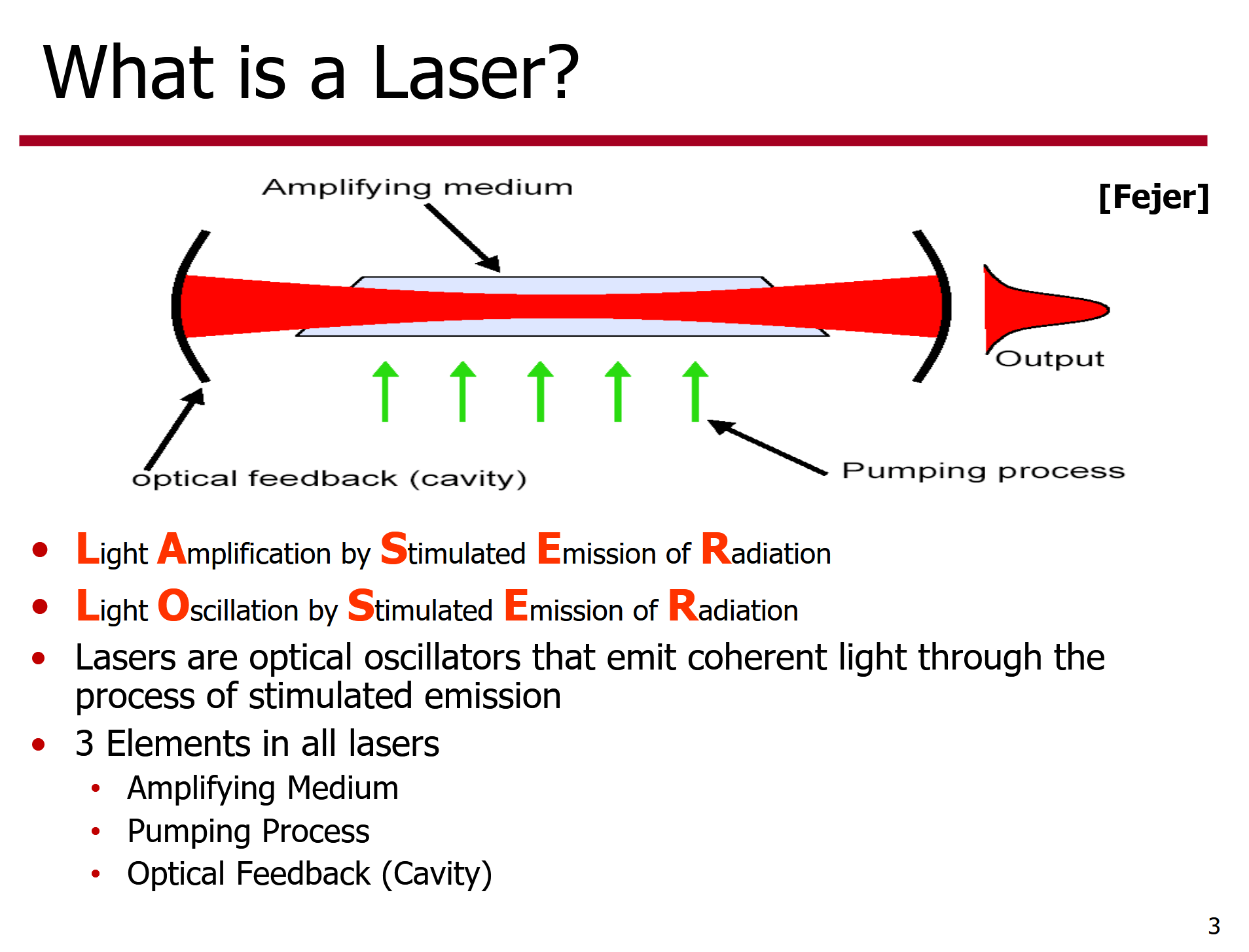
Silicon is terrible for building lasers. The material of choice is either Gallium-Arsenide or Indium-Phosphide.
Vikram Sekar covered this topic very well.

There are a wide variety of laser types. Keep in mind that each of these emits a single wavelength of light. One carrier wave.

For generating multiple wavelengths of light, there are three broad categories of solutions.
Laser Arrays
Put many lasers of different wavelengths on a single chip.
Alternatively, combine an array of lasers using an external waveguide.
Terrible reliability and huge power draw.
Quantum Dot
Use specialty process tech.
Terrible yield.
Kerr Comb
Use nonlinear phenomenon to split light into multiple wavelengths.
Terrible energy conversion efficiency.
Generating multiple wavelengths of light is a major challenge.
[3] Photodetectors
Photodetectors convert light into electrical signals.

A lot of this stuff is materials science and physics related so I want to avoid writing about it.
What matters from a communications systems perspective is the optical to electrical (OE) conversion efficiency and noise performance.
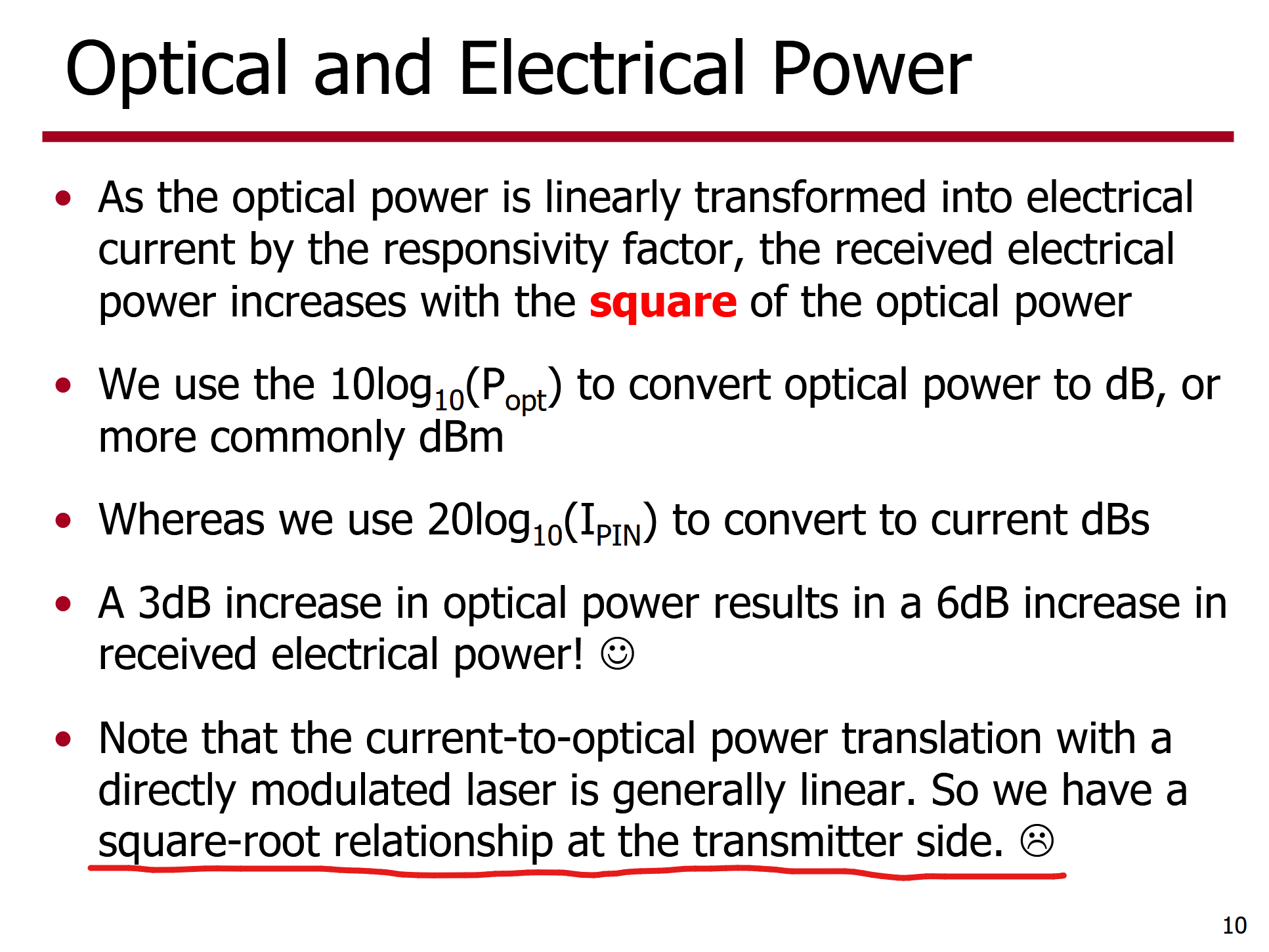
It is easy to juice receiver electrical output with stronger light. However, that requires very large power boosts on the transmitter.
The key point is…
Laser noise performance and linearity at high power is the limiting factor, not the photodetector.
[4] Modulators
Think of modulation as “encoding binary data onto an analog carrier signal”.
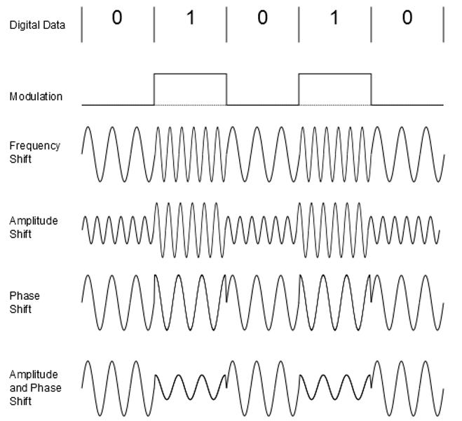
There are several types but co-packaged optics tends to use amplitude shift based modulation.
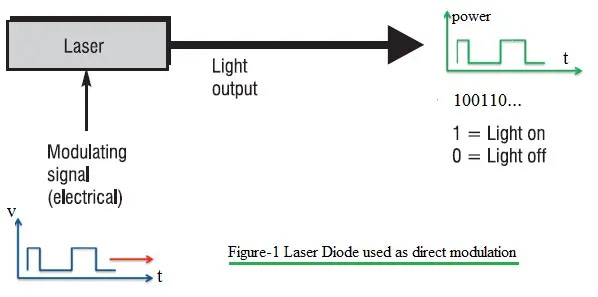
[4.a] Direct Modulation
Direct modulation occurs when the power source to the laser acts as the modulation mechanism.
Pros:
Cheap.
Easy to design and implement.
Cons:
Severely bandwidth limited.
Horrible reliability.

[4.b] External Modulation
External modulation uses a silicon-photonics device to modulate a continuous-wave external laser.
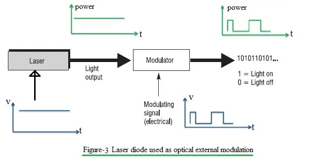
Pros:
Can support multiple wavelengths in a single PIC.
Bandwidth not limited by laser.
Cons:
Optical insertion loss.
Modulator tuning and stability.
Yield issues from fiber attach.
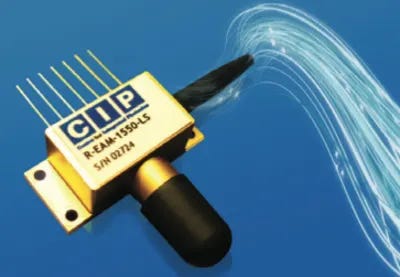
[4.b.i] Electroabsorption (EAM)
Electroabsorption modulators look like this.
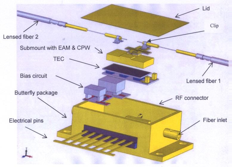
These are chunky devices traditionally used in telecom applications where space is not an issue. The reason is reliability.


Switching voltage from 1.5V to 4V is not a good thing.
Modern process nodes cannot deal with such high voltages.

This tech is not viable for CPO or datacom in general. The modulation is too weak and the reliability is horrible.
[4.b.ii] Mach-Zehnder (MZM)
MZM use phase shifting to destructively interfere a signal to a logical zero.
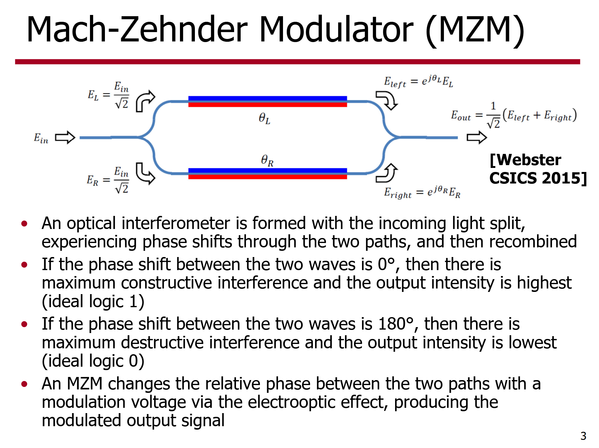
These devices work very well but have two major flaws:
Take up a lot of space.
Meaningful insertion loss.
MZM loss in a normal topology is not an issue. However, a DWDM topology with many wavelengths cannot easily chain MZMs in a row.
In other words, a chain of 8+ MZMs on the same waveguide will induce way too much optical insertion loss.
[4.b.iii] Micro-Ring Resonators (MRM)
MRMs are special because they enable massively scalable systems on a single fiber.
Each of the rings modulates a single wavelength of light. Insertion loss is minimal. You can chain these devices very aggressively.
Intuitively, you can think of a MRM as an optical notch filter.

And it is helpful to directly compare MRM with MZM.

Wavelength sensitivity == thermal stability
So lets talk about the circular elephant in the room.

Micro-rings are very sensitive and need to be controlled with tiny heaters.

Those of you who work in the semiconductor industry might be thinking…
“Wow… controlling sensitive devices with heaters sounds very difficult.”
You are right. This shit is a nightmare.

If the temperature is not just right, the modulation strength (aka extinction ratio… aka “how different a logical 0 is from logical 1” goes WAY DOWN.
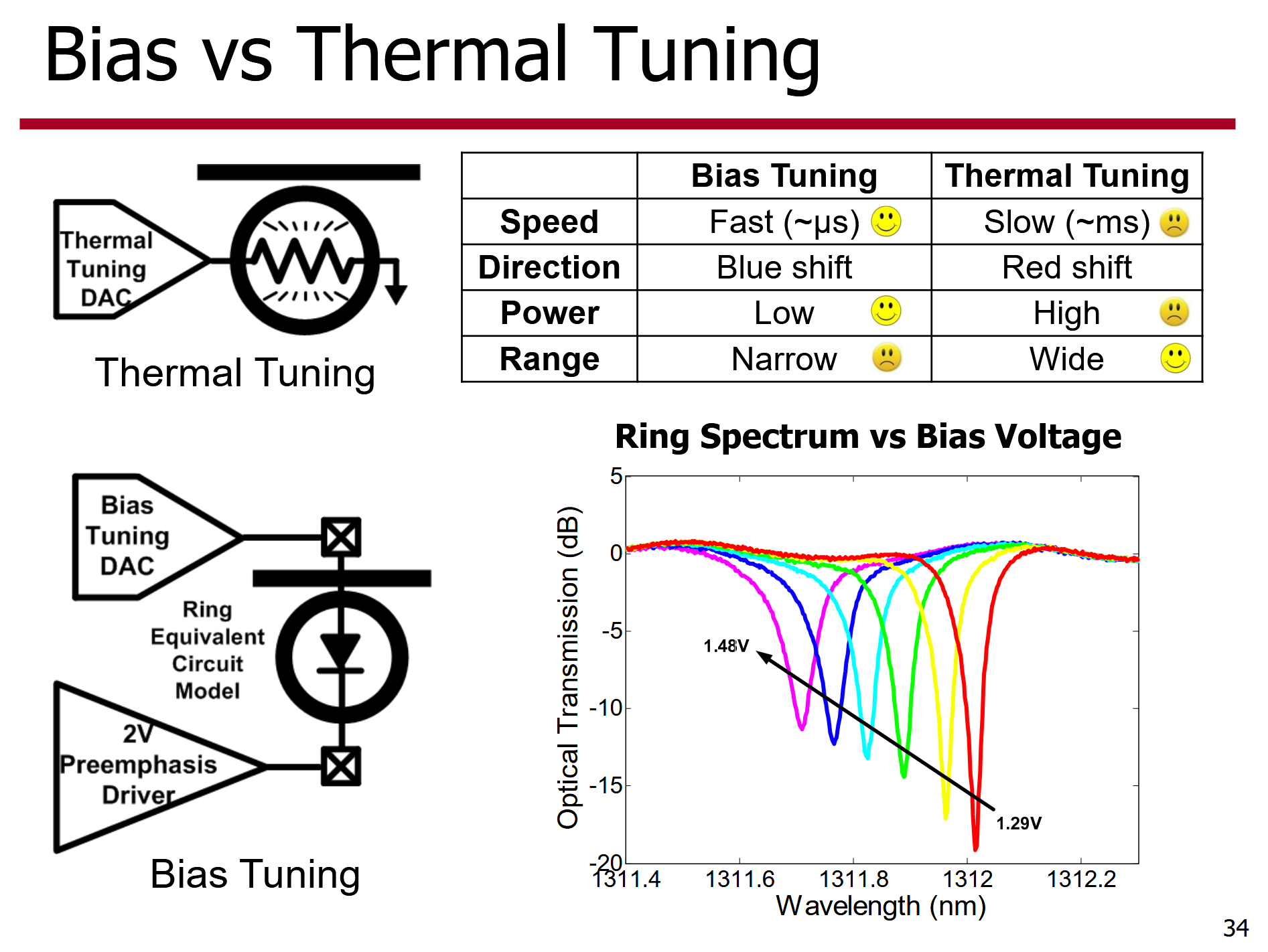
MRMs are incredible relative to MZM in every way EXCEPT for stability.
Solve the stability problem and you win.
[5] Two Tribes and a False Choice
The optics world is divided into two tribes.
Clan Micro-Ring and Clan Mach-Zehnder each tell the outside world the other tribe are morons.
Mach-Zehnder modulators are too large and have significant insertion loss, Clan Micro-Ring screeches.

Micro-Rings are too thermally unstable, shouts Clan Mach-Zehnder.

This is the false choice presented to investors and prospective employees.
Don’t fall for it. Dig deeper.
It’s based on a technology called micro-ring resonator modulator. (MRM)
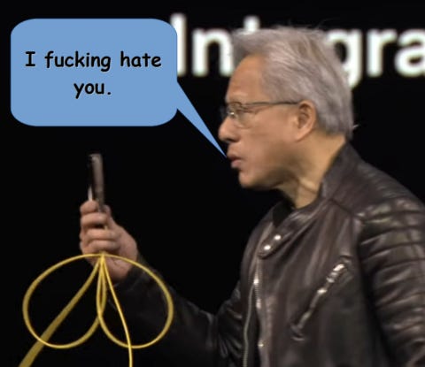
Now the reason we decided to invest in MRM is so that we could prepare ourselves using MRM’s incredible density… better density and power compared to Mach-Zehnder which is used for telecommunications.. when you um uh drive from one datacenter to another… or even in the transceivers we use… we use Mach-Zehnder because the density requirement is not very high… until now.
-Mr. Leather Jacket, GTC 2025
Both technologies are viable for CPO. The engineering challenges are very different, which is why each tribe so aggressively shills their choice. Once a company makes a choice on modulator, they are basically committed.
Rings are really damn unstable. Thermals are a huge problem.
Notice something about Nvidia CPO?

The switch chip itself is liquid cooled. Photonics IC (aka PIC aka photonic engine) is far away, surrounded by a block of aluminum. This chunky heatsink is there to absorb and slow down thermal variation induced by the switch chip.

Mach-Zehnder is thermally stable but now you have to make a make a lot of changes to the package design.
https://en.wikipedia.org/wiki/False_dilemma
[6] Electrical Periphery: TIA and all that
I often see sell-side research notes discuss TIA (transimpedance amplifier) as if this thing is some kind of discrete optics-specific component.
TIA is a basic circuit that has many applications.

Electrical SerDes often have multiple TIAs as a part of their CTLEs.
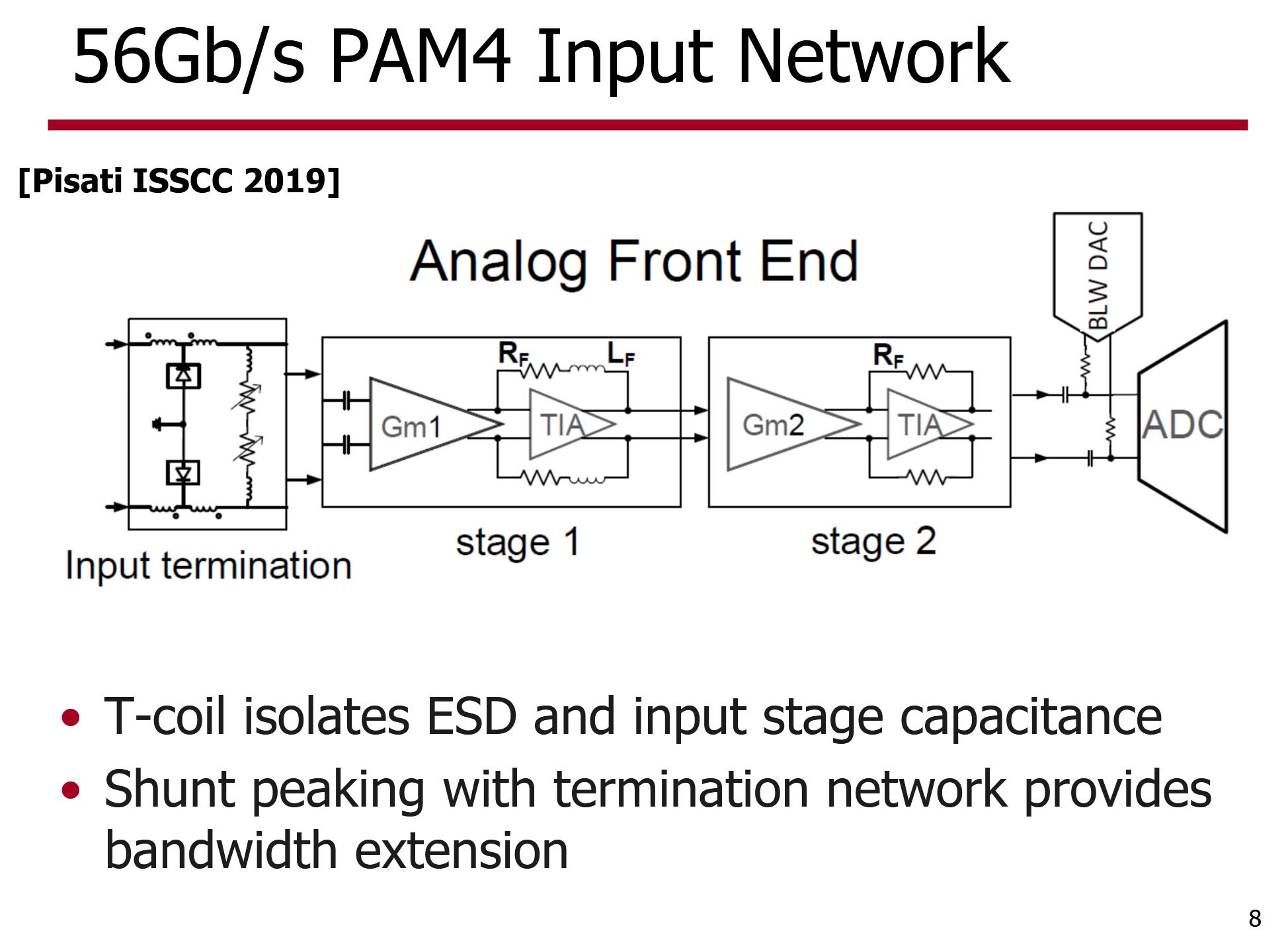

Would you look at that! Basically every high-speed system has multiple TIA integrated on die. It’s almost as if TIA is a basic circuit and not some kind of magic optics-only discrete component.
In general, optical systems need a series of electrical amplifiers to deal with low electrical output from the photodetectors/photodiodes.
The amplifier chain tends to follow a similar structure across designs. For example, a TIA followed by a main amplifier that likely has automatic gain control (AGC).
Managing noise across the amplification chain is important. Integration helps with mitigating the effects of parasitics.
[7] Incorrect Obsession with Silicon “Beachfront/Shoreline”
I see many people (engineers and analysts) obsess over beachfront and shoreline.
We are limited by bandwidth per silicon/die millimeter, they screech.
This take is extremely wrong.
Go ahead and pack together SerDes lanes on silicon. Your system will have dogshit performance because of crosstalk at the package level.
Here is a snip from a TSMC paper on integrating UCIe on CoWoS-R.

Crosstalk at the package kills performance.
Package cost (many high-speed signal layers) kills gross margins.
At 200G speeds, most of the link margin is eaten just from the package.
Why, you might ask?
It’s because of the skin effect.
Also the fact that most packaging technologies cannot build proper ground shields.
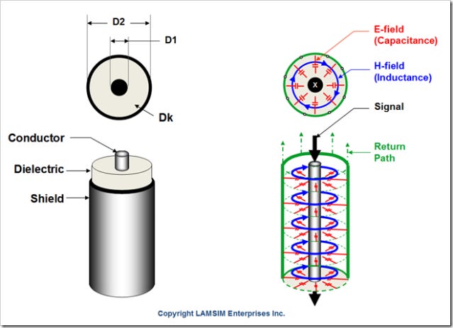
Ideally, you want ground to uniformly surround the signal wire.
This is not possible on most packaging tech.
As a workaround, package and PCB designers use tricks.
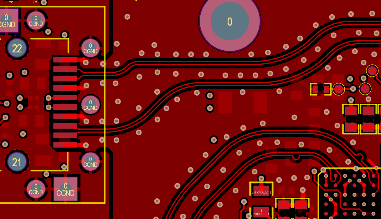
See all those dots next to the traces? Those are vertical VIAs that connect to ground planes.
It’s a ghetto way of building a partial coax ground shield.
Two planes with many vertical pillars connecting them together.
Anyone who claims that silicon beachfront/shoreline is the I/O limit does not know what they are talking about.
**Package crosstalk is the limit.**
[8] Photonic Process Nodes
Photonics nodes tend to be around 45nm to 65nm class.
This is because optical structures (modulators, waveguides, photodiodes) tend to be large. Scaling sucks. It’s like analog scaling but so much worse.
Global Foundries has a 22nm-class photonic node called 22FDX.

It was launched in 2015 and still nobody fucking wants to use it.
It’s too expensive.
Photonic process nodes also have terrible PDK relative to logic nodes. I have had several “wait they don’t provide you with this info” conversations.

[9] Walkthrough: Nvidia Quantum-X GTC 2025 Announcement
Previously wrote a low-quality news post:
Now that I have had time to properly explain the technical background, let’s go over this again.
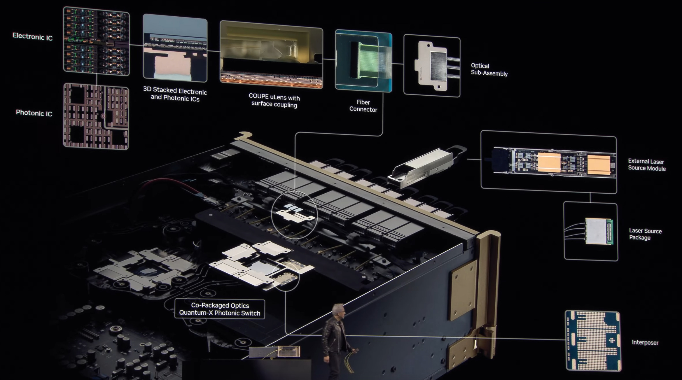
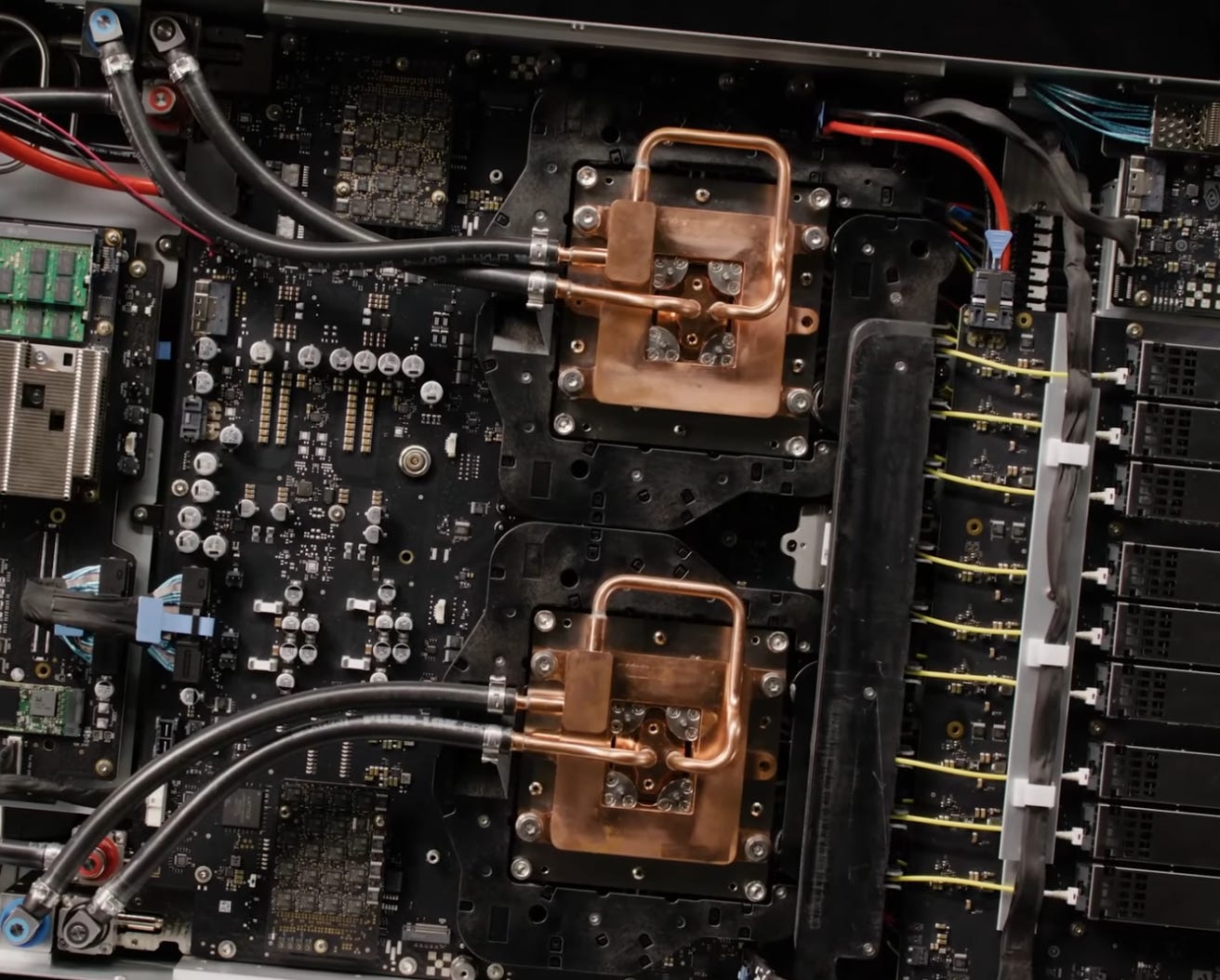
Liquid cooling of the switch chips.

Chunky aluminum heat shields to protect the ring modulators on the photonic ICs.


They are directly driving the rings at 200G PAM4. This is interesting because the frequency response of MRMs is not good. Nvidia likely had to use agressive pre-distortion to get this to work.

TSMC N6 is for the EIC. The PIC is likely TSMC 65nm based on some papers I found.

It’s a laser array. You think this shit is reliable? LOL
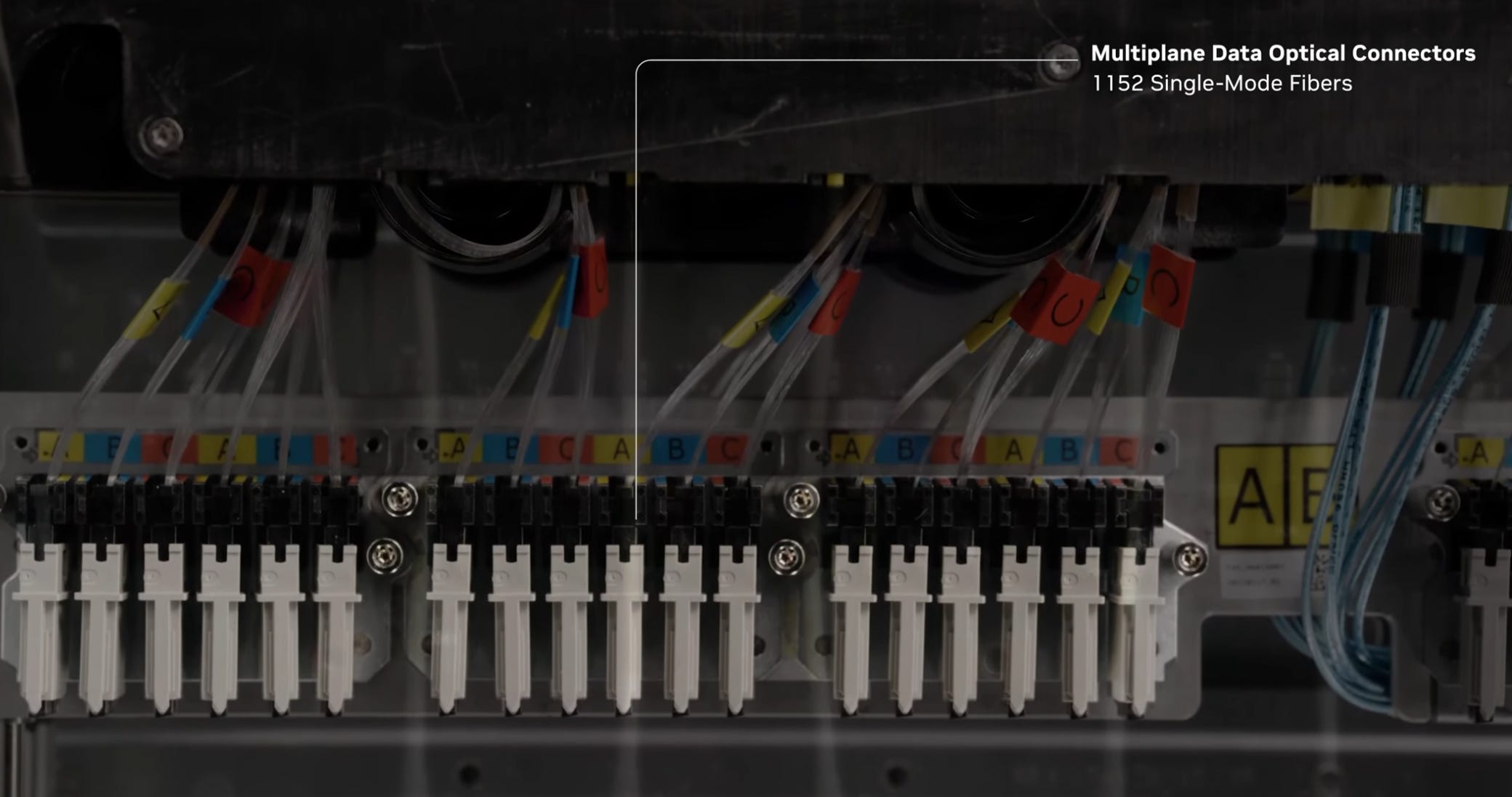
Having 1152 fibers in your system is not a good thing. Nvidia is limited by the number of wavelengths from the light source. A 16-lambda laser could cut fiber count in half-ish.
[10] Walkthrough: Broadcom Hot Chips 2024 Baily Presentation
I previously covered Broadcom’s CPO presentation at Hot Chips 2024 here:
Understand the tech much better now so lets try again.


Structurally, Broadcom’s solution is similar to Nvidia’s.


Unlike Nvidia, Broadcom did not use COUPE (TSMC hybrid bonding). Instead, they used a cheaper RDL-based packaging tech. I expect them to move to COUPE for next generation.

TDECQ of 1.07 dB is kickass.

No errors past RS-FEC symbol 5, with further optimization likely achieved by now.
Unfortunately, the presentation had very little information on the PIC itselft.
I suspect Broadcom used MZM. If they were using rings, they would have bragged about it.
[11] Public Market Investment Corner
This is not meant to be an exhaustive overview of all companies involved with CPO. Only companies I am aware of and interested in covering are included.
[11.a] Transceiver Exposed Companies are Fucked
Any company that has significant revenue exposure to optical transceivers is fucked. The entire point of CPO is to remove the transceivers…
[11.b] oDSP Exposed Companies also Fucked (COUGH COUGH MARVELL)
A huge portion of Marvell’s revenue is optical DSPs from their Inphi acquisition.

THE ENTIRE POINT OF CPO IS TO GET RID OF THIS PART.
https://www.marvell.com/products/pam-dsp.html

My gut feeling is this business revenue peaks in 2025 and declines by 50-70% by 2030.
[11.c] CPO Developers: Nvidia, Broadcom, and Marvell
Nvidia and Broadcom both have excellent CPO solutions.
Marvell’s solution is dogshit.
I went to the MRVL 0.00%↑ booth at OFC and gently asked some questions about their vaporware CPO mock-up. Knew all of the answers already. Just wanted to pretend to be an idiot and get the marketing dude to dig his own grave by confirming my priors.
They don’t have anything.

I call their bluff.
Marvell had profound “loser energy” at their OFC booth.

Attractive funding short in semis.
[11.d] Laser Manufacturers: Lumentum and Coherent
Both of these companies make a variety of lasers. They both also have sizable transceiver businesses.
Just because Mr. Leather Jacket showed their logos at GTC does not mean these tickers are good investments.

[11.e] Outsourced Assembly: Fabrinet (is better than everyone else)
I have covered Fabrinet multiple times. Go check out old posts.
They are exposed to transceivers, but are uniquely positioned to gain overall share with CPO.
Co-packaged optics involves a lot of sensitive IP. This is not the kind of shit you want to share with Eoptolink or Innolight…

Fabrinet is a trusted manufacturing partner within the industry. They literally segregate cleanroom space and employees for each customer.
[11.f] Glass: Corning and Nittobo
You may be familiar with Corning from the “Gorilla Glass” product inside basically every smartphone.
They have a huge optical communications fiber depeartment.
Nittobo is a Japanese company that makes ultra-low loss glass fiber. Given the shitshow that is going on right now, I am seriously considering buying some foreign stocks just to get exposure to “anything other than USD”.
[11.g] Fabs: TSMC War Against GloFo and Tower Semi
Traditionally, Global Foundries and Tower Semiconductor are the Fabs that have good photonic process nodes.
TSMC has a photonic node and it sucks. This is not my opinion. It is the opinion of MANY people across MANY companies who I have spoken with.
Mr. Leather Jacket shilling TSMC photonics node is a publicity stunt.
The problem is, COUPE (TSMC tech for hybrid bonding PIC and EIC) and TSMC advanced packaging (CoWoS-L) are fucking amazing.
TSMC has a policy of refusing to advanced-package chips from other fabs.
This policy is “encouraging” many companies to ditch Tower/GloFo and use TSMC for their PIC instead.

COUPE has incredible return loss. Also basically zero insertion loss.

Ultra clean power supply. Basically no ripple.

CoWoS-L has incredible insertion loss. Less than 2 dB at 53 GHz. This is nothing. A normal package easily hits 8 dB insertion loss under the same conditions.
CPO using COUPE and CoWoS-L can easily achieve less than 3 dB of insertion loss with exceptional crosstalk isolation.
TSM 0.00%↑ photonics process node sucks but COUPE and CoWoS-L creates an incredible moat. GFS 0.00%↑ and TSEM 0.00%↑ shareholders beware.

so what do you think the timeline for mass CPO adoption is? and when do we get it in scale up vs just scale out? great writeup as always
Gosh , you are funniest technical genius . Superb , plain old superb . Kudos Sir