IMPORTANT:
Irrational Analysis is heavily invested in the semiconductor industry.
Please check the ‘about’ page for a list of active positions.
Positions will change over time and are regularly updated.
Opinions are authors own and do not represent past, present, and/or future employers.
All content published on this newsletter is based on public information and independent research conducted since 2011.
This newsletter is not financial advice, and readers should always do their own research before investing in any security.
Feel free to contact me via email at: irrational_analysis@proton.me
Hot Chips is an annual semiconductor engineering conference. A three-day event with lots of exciting presentations from large companies, academia, and startups.
I will cover all interesting portions of the conference in this post, loosely grouping and ordering presentations by sentiment.
Note: You should probably read this one from a web browser. Email will almost certainly be clipped.
Excellent
Broadcom Co-Packaged Optics
Meta Recommendation Inference ASIC
Tesla Transport Protocol — Ultra-Dumb NIC
Good
Qualcomm Oryon CPU
IBM Telum 2
Tutorial: AI for Hardware Design
Tutorial: Liquid Cooling
Poster: Radix-8 FFT Accelerator
Meh
Intel Lunar Lake
Intel Edge Xeon
Enfabrica
Intel Silicon Photonics
SambaNova
FuriosaAI RNGD
Frore AirJet
Bad
Tenstorrent
Nvidia Blackwell Advertisement Re-run
Literally Every Single AMD Presentation
Cerebras Inference Pipedreams
Microsoft Maia
Intel Gaudi 3 (is already dead)
Tutorial: Qualcomm On-Device AI
Phononic Solid-State Cooling
Dumpster Fire
Ampere Computing
SK Hynix In-Memory Compute
Terrifying — Trevor Cai, the OpenAI Guy
Excellent Technical Material
“Sometimes lines really do go up”
Solar Panels
Moore’s Law
Surreal Bubble Inflation
Winners and Losers
[1] Excellent:
Excellent presentations deserve special commendation for a combination of rich technical material, high-impact products, and overall delivery.
[1.a] Broadcom Co-Packaged Optics
Prior to this presentation, co-packaged optics were a 2028 technology in my opinion. Broadcom’s incredible presentation changes everything. It looks like 2026 high-volume production is highly likely.
Reliability and serviceability have always been a major concern with CPO. Broadcom has moved the laser source to a pluggable front-end as that is the most failure-prone component. It also has temperature sensitivity which can be adequately controlled/cooled in the front panel. The presenter exuded confidence that this form of CPO (front panel laser, everything else integrated) is meets reliability and serviceability requirements for massive scale deployments.
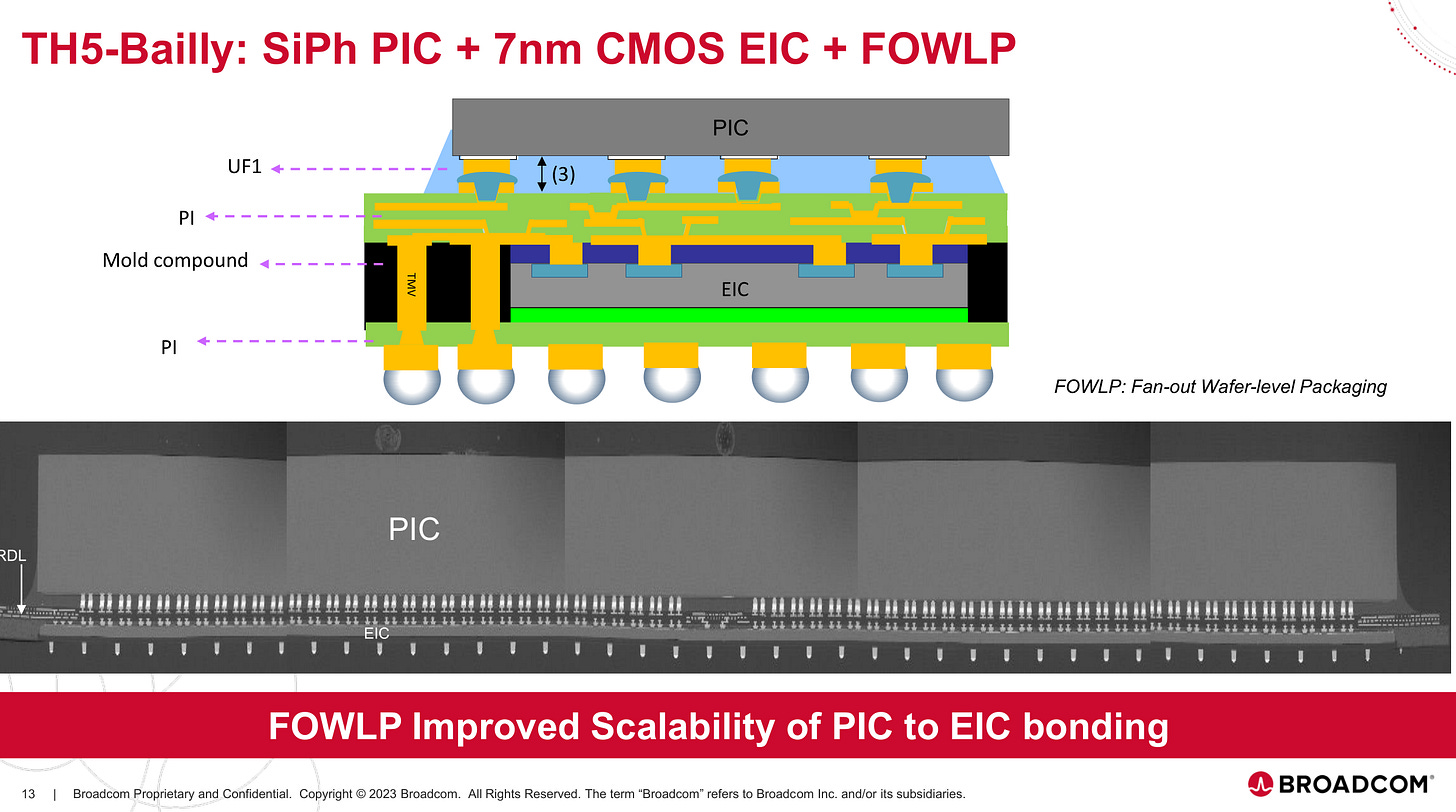
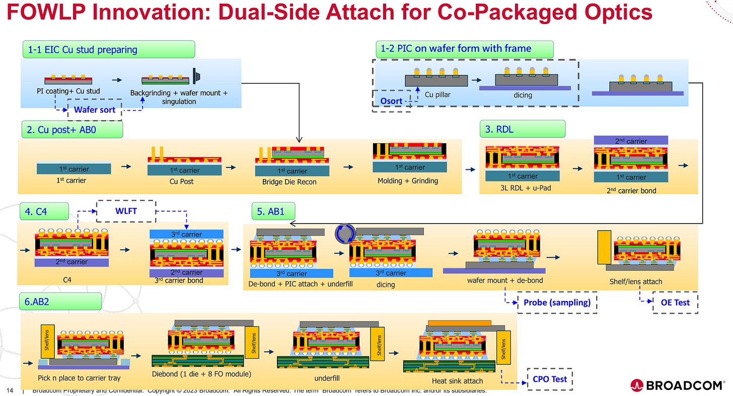
All the photonic components are integrated into a photonics IC (PIC) and hybrid-bonded to the electrical IC using Fan-out Wafer-level Packaging. Yields are apparently very good.
Importantly, everything on the package is silicon. The process node for the PIC and EIC are of course different, but both are silicon-based processes. Manufacturing, packaging, and test are all mature, leading to high yields.
Look at how clean these SEM cross-sections are!
CPO enables much higher radix (number of ports per switch chip), allowing for simpler network topologies. Less layers in the network means massive cost and power savings.
The demo is incredible. They did not try to hide minor flaws. Transmitter linearity is failing (needs to be >= 0.95) and they still showed the results! Eye is super clean considering every lane is in loopback and active, acting as aggressors dumping noise into the lane under test. Power of 4.8 watts per lane is super amazing.
FEC data for every single port on a production-quality part!
They even showed some optimized in-progress lab results where they almost have threshold 3 error free.
Suppose you have a link with a raw bit-error-rate (BER) of 1e-8. With forward-error-correction, you want to get that to 0, error free, even if there are burst errors in the system. This is very difficult. High-speed Ethernet SerDes typically use Reed-Solomon error correction which can be configured.
A heavy FEC configuration adds more parity data, reducing use-space data transmission but enabling greater error detection and correction capabilities.
Ideally, you want the physical layer (PHY) to be as error-free as possible to enable running a lighter FEC config, providing more usable data bandwidth.
Broadcom has shown that with some lab optimizations, they only have two ports with uncorrectable errors at symbol threshold 4, with the rest at symbol threshold 3.
This is very good. If they get all ports to 0 uncorrectable (error free) at symbol threshold 3 then this product is ready for high-volume production.
I cannot overstate how kickass this is. They are showing real, high-quality, raw data and saying, “yea we gona fix this in ~1 year and crush all you fools”.
This news is terrifying for MRVL 0.00%↑ , who is heavily dependent on oDSP revenue.
[1.b] Meta Recommendation Inference ASIC
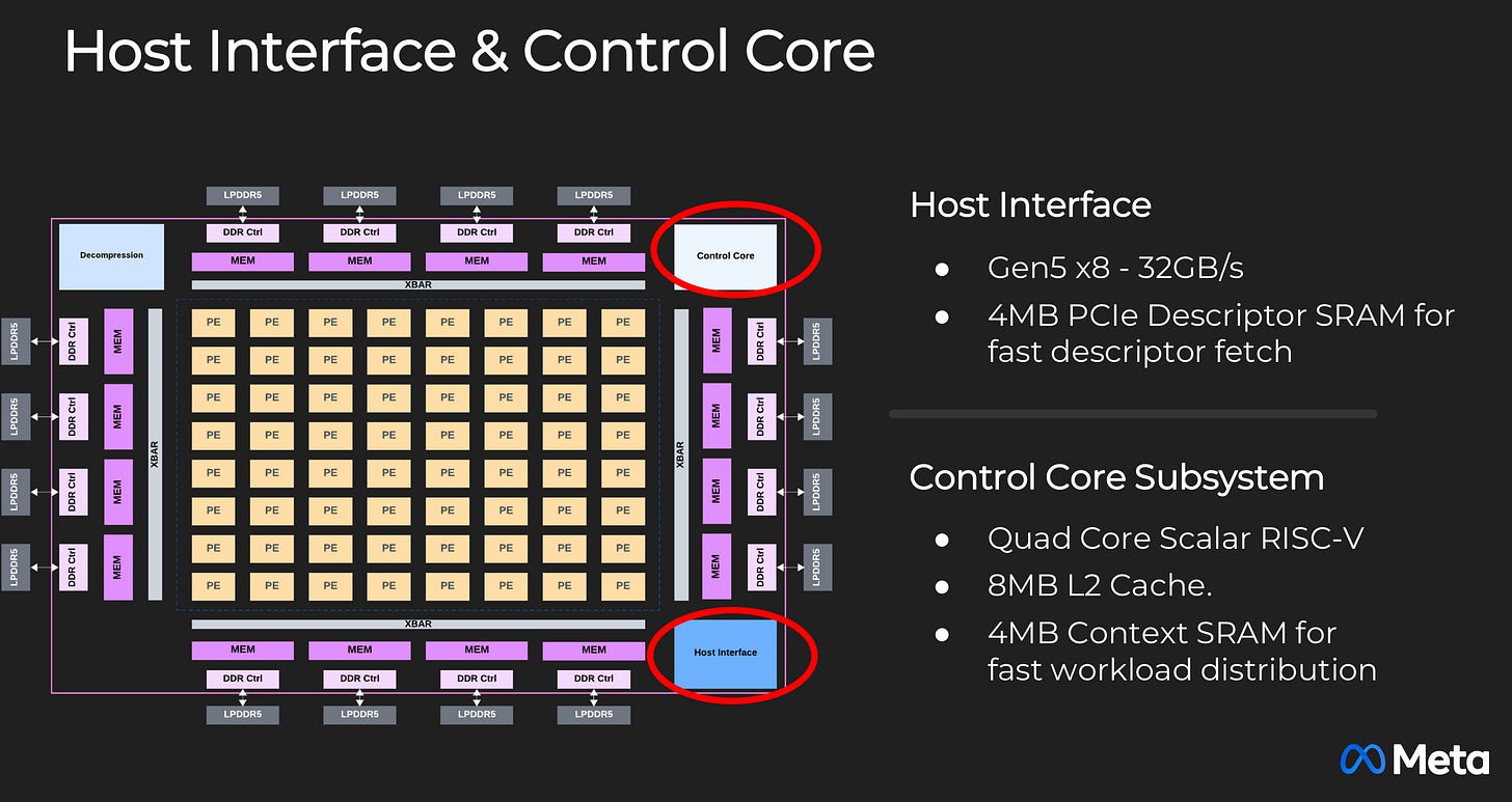
This chip is designed to accelerate recommendation network inference. A major feature of recommendation networks is the large embedding tables. Basically, this Meta chip is a true ASIC, extremely cost-optimized, high-performance inference of once specific flavor of neural network, not that good for anything else.
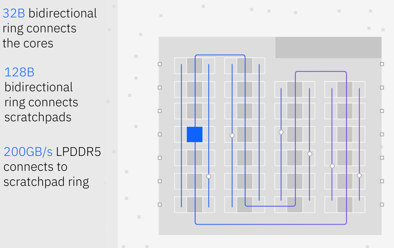
Notice the LPDDR5. They have a brilliant solution to this bandwidth bottleneck while maintaining the cost and power savings enabled by LPDDR vs HBM.
Very heavy on the SRAM. Custom mesh.
Cheapo RSIC-V control cores to save money and avoid paying the ARM tax. Good move for such a cost-optimized, internal-only chip.
Both the PCIe PMA and RISC_V CPU cores get a nice chunk of dedicated SRAM to make sure workloads are configured quickly.
There are two networks-on-chip (NoC), one for data and another for configuration. This is surprising. Never seen this before. Physical design routing of these two NoCs (both have to connect to each processing element) must have been challenging.
Dedicated data and config NoCs probably help a lot with the programming model. Don’t have to worry about collisions between kernels and data.
RISC-V again for maximum customization, power saving, and not paying money to ARM 0.00%↑ in a cost-optimized, internal-only project.
There is hardware-level support for some micro-quantization. It is unclear if these are MX compliant. In Q&A the presenters admitted that none of these fancy quantization methods are currently in use within Meta’s production datacenters even though the chip was put into production in Q1 2024.
In order to compensate for the mediocre bandwidth of LPDDR5, Meta added a dedicated on-die decompression engine. Super-lossless compression at a 50% ratio.
Accelerators and compress, transmit, and decompress data to one another at lightning speed over PCIe because of the hardware compression engines. CXL-based memory expansion adds an additional giant pool of memory.
Some hand-optimization of data blocking within SRAM partitions is needed to squeeze all the performance out of this chip. This is likely why the control and data are on dedicated NoCs.
[1.c] Tesla Transport Protocol — Ultra-Dumb NIC
Before getting into the presentation, I want to take a moment to call out the speaker himself, Eric Quinnell.
Without a doubt, he was the best presenter at Hot Chips 2024.
High energy delivery.
Comedy routine.
Multiple really funny jokes that got audible laughter from the audience.
Self-deprecation that hammers-home the objective of TTPoE.
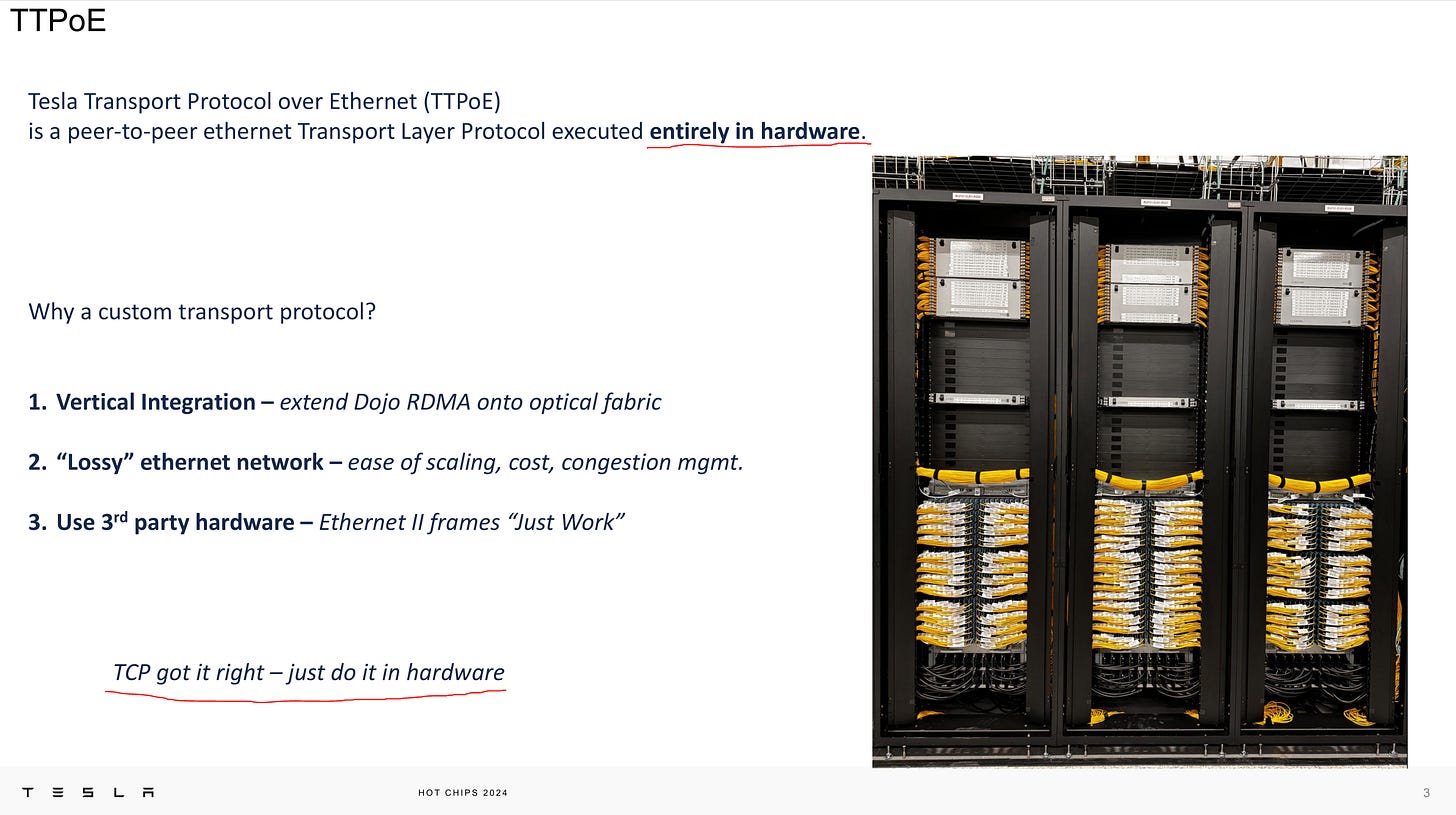
Brought props on a table to show everyone what the hardware looks like.
Excellent technical explanation.
A hardware-based TCP implementation… interesting. How?
A state-machine implemented with physical memory only on a cheap-ass FPGA.
Some banger lines from the talk:
Dojo lost its Mojo.
We want the dumbest NIC. No OS, no CPU cores, no nothing.
PCIe Gen3 x16 is enough to push 100Gbps Ethernet and is cheap. We love cheap.
DDR4 is cheap. Cheap is great.
We want to sprinkle these dumb NICs everywhere. SO CHEAP!!!!
This solution is cost optimized, awesome, and hilarious.
These ultra-dumb NICs act as nodes on the DIP (Dojo interface processor) network to allow flexible scaling.
They have a 4 exaflop engineering/testing system. LOL
Donating the spec to Ultra Ethernet! Bravo!
The latency bar chart is on log scale. Absolutely crushed the design goals. Congratulations to every person who worked on this feat of engineering.
[2] Good
Good presentations offered useful information and/or shared technical details on quality products.
[2.a] Qualcomm Oryon CPU
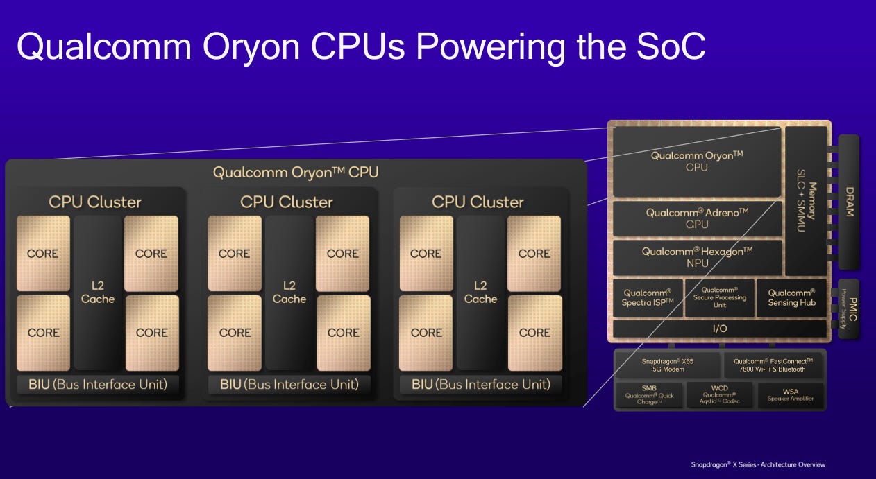
One neat tidbit is one of the CPU clusters is “different in its physical construction” to enable better power efficiency.
Seems like efficiency-focused transistor libraries and standard cells were used for the efficiency cluster, even though the higher-level RTL is the same.
Use different physical design blocks, sacrifice FMAX for better power efficiency.
The inner workings of this forwarding mux would be interesting.
Each core typically uses 3-4MB of L2 at runtime but can use more if needed. Latency of 15-20 cycles.
[2.b] IBM Telum 2
Why do mainframes still exist?
To process financial transactions in real-time with ultra-low latency and absurd uptime/reliability.
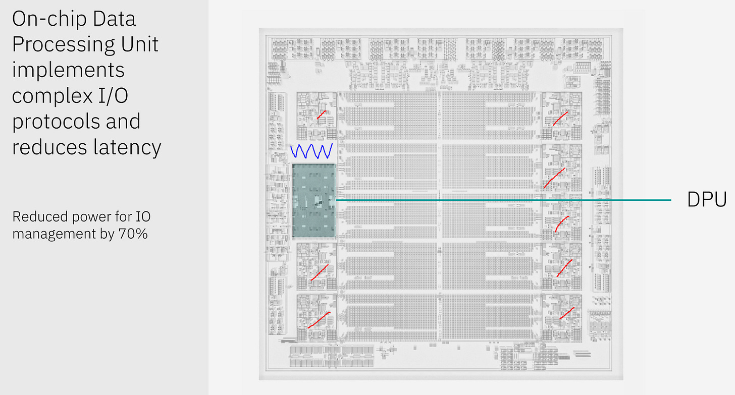
Previously, IBM would include extra cores to improve yield. In this generation, they decided to remove two extra/spare cores and plop in a dedicated DPU. There is some dead space (blue squiggle) which is unfortunate but overall smart design choices.
This built-in DPU is pretty nice. Enables L2 coherence across 32 Telum II chips. IBM chips have a fancy virtual L3 and L4 system. Speaking of virtual cache…
Each CPU core can access all the other L2s as a virtual L3. They can even access other chips L2 as a virtual L4. This feature is unique to IBM chips and is very cool, especially given all of these virtual cache accesses support cross-node encryption.
Unfortunately, IBM did not share the expected latency for DDR5 hits. Presumably, the latency would be somewhere in the 80-120ns range so a virtual L4 hit is still better than a local DDR hit.
The previous generation had an on-chip AI accelerator, and it has gotten significant upgrades. Note that the LLM commentary is marketing hype. Nobody is gona use this thing for LLMs lol.
Interesting that they have choses a CISC uarch and rely on ML op fusion. Can’t think of anyone else who has gone this route.
One important new feature that was verbally mentioned is each CPU core can access every AI accelerator within the same drawer, with a latency penalty of course. Only one CPU core can use the AI accelerator at a time and customer use has steadily increased. To mitigate congestion issues, cross-chip AI accelerator access was added. It’s a good sign. IBM’s customers (banks, credit card processors) are actually using the accelerator.
They put 32 copies of this AI accelerator on a dedicated chip. Not sure who is going to buy this.
Marketed as a genAI solution. Hard doubt on this one. Maybe some of the financial institution customers will buy some of these to make bizzarro AI trading bots. The software stack and architecture are too bespoke (painful to program) for anyone outside of IBM’s existing customer base to bother with. Accumulation and activation ops seem to be handled in a rather rigid manner, especially in the context of data precision. When you see “scratchpad” think programmer-managed memory… AKA painful programming model that has a high-skill ceiling to achieve advertised performance. Someone at Citadel is gona have a lot of fun with this Spyre chip.
[2.c] Tutorial: AI for Hardware Design
There were multiple, excellent talks on using AI for chip design that I will lump together in this section.
Cross-stage analysis and optimization is very important, given how complexity of leading-edge chiplet systems has exploded.
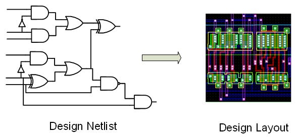
Physical design optimization is well-suited for conv-nets. Simulating IR drop (intrinsic resistance/impedance of each sub-circuit) is very slow. AI helps by estimating where problems are likely and allow experienced designers to target EDA analysis tools on specific portions of the chip.
Analog circuit design is typically in two discrete stages:
Make a schematic of the circuit.
Implement the schematic on a physical design.
“Parasitics” refers to unwanted attributes. Typically, resistance and capacitance.
Examples:
Wires have intrinsic resistance. If you don’t account for this, the voltage drop might be too high resulting in bit-flips/errors.
Devices (transistors, diodes, flip-flps,…) have intrinsic capacitance that can easily mess up your transient response.

The normal way to handle these problems involves a lot of back-and-forth. It is somewhat challenging to have physical designers and circuit/schematic designers bounce design revisions across their fields. Using AI to predict possible parasitic issues is a great productivity boost for both departments.
Commercial EDA tools have macro placement tools but the configuration parameters for said tools have a huge impact on output quality. The baseline is for experienced designers to guesstimate what parameters to choose, run the tool, analyze the results, then try again.
AI once again provides a massive productivity boost. More coverage of a wider search space and faster iteration to a better end-result.
Modern process nodes have many design rules. A reinforcement-learning AI agent can automatically play a “game” that removes DRC violations.
Reinforcement-learning has many other uses. Any optimization problem with a clearly defined environment, reward mechanism, and large search space is quite well suited for RL.
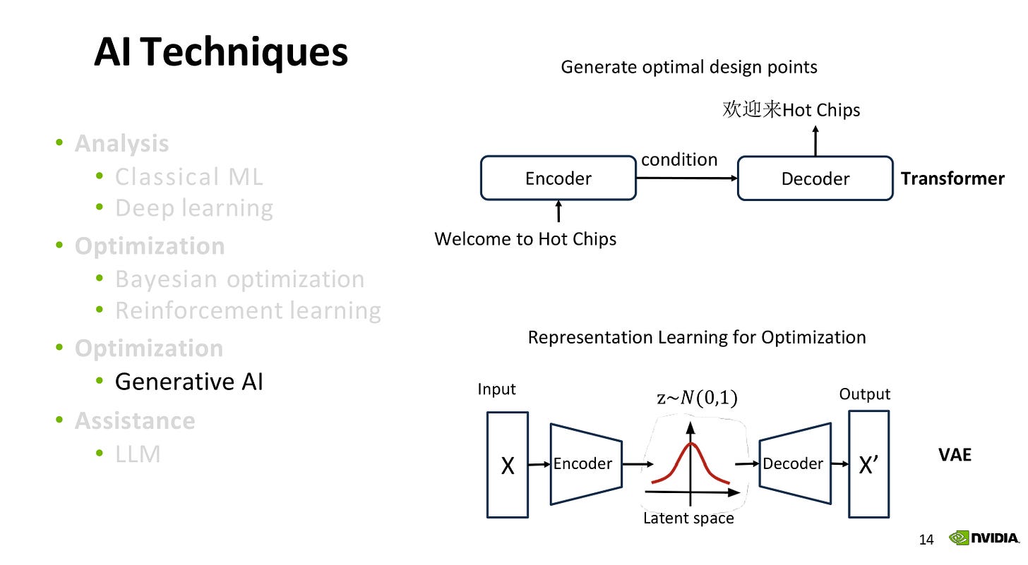
On to the modern (bleeding-edge) techniques. Generative AI (transformers) is very good at compressing massive search spaces into an intermediate representation, latent space, allowing for efficient analysis of pre-filtered optimization points.
One example is logic gate sizing. The search space for optimizing power, area, and performance (delay) for individual logic gates is massive. By tokenizing each gate in a circuits critical path, the transformer optimizer can quickly find optimization opportunities. An incredible 2-3 order of magnitude speedup was achieved compared to traditional EDA optimization tools.
At this point, the Nvidia presenter not so subtly took a jab at the EDA vendors for being too slow to implement new features. If a customer can develop a 100x to 1000x faster optimizer, you might be innovating too slow.
Once again, the latent space of a transformer model is very good at choosing optimizations of complex designs with very large search spaces. A dimension-reducing function to search faster and find better local minima/maxima.
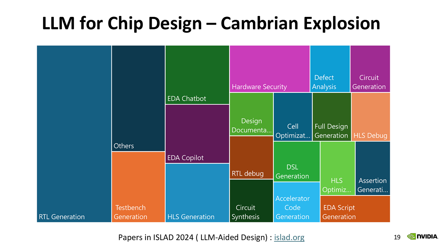
LLM agents are generalists that can be RAG-ed onto internal proprietary data. Simulations, custom standard cells, past chip designs, …
Most of the focus has been on RTL generation but the presenter went out of his way to highlight that LLM agents are super useful across a wide variety of domains. Bug report analyst, testbench assistance, EDA script generation, … we have only scratched the surface of chip design productivity improvements with LLMs.
On to the Synopsys presentation.
Design search space is massive and gets exponentially larger at each step of the process.
Complexity harms productivity, and thus cost.
Identifying cross-layer optimization opportunities is very difficult but critical to squeezing out every competitive advantage possible.
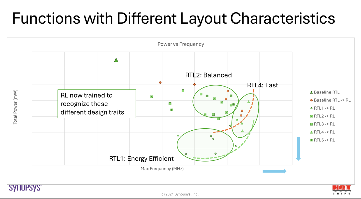
Reinforcement learning once again comes in to save the day. In this plot, the bottom left is desirable. Goal is to minimize leakage (wasted) power and TNS (total negative slack), a measure of timing violations. The RL/AI agent out-performed months of human work by 30%.
In this example, the yellow triangle is the human-designed baseline. AI/RL floor planning found multiple solutions that not only improve on the human design but also offer optionality. Could optimize for area (cost) or performance or both. Regardless, these new options are enabled by the RL agent. Many engineer-hours of human work missed all these options because the design space is simply too big.
Multiple RL agents can be trained with different reward mechanisms, leading to different results. Lots of way to set up the game.
[2.d] Tutorial: Liquid Cooling
Fun-fact, one of the circuit breakers at Stanford tripped as the Supermicro presenter was talking about power limitations. The market happened to crash on that day. No correlation.
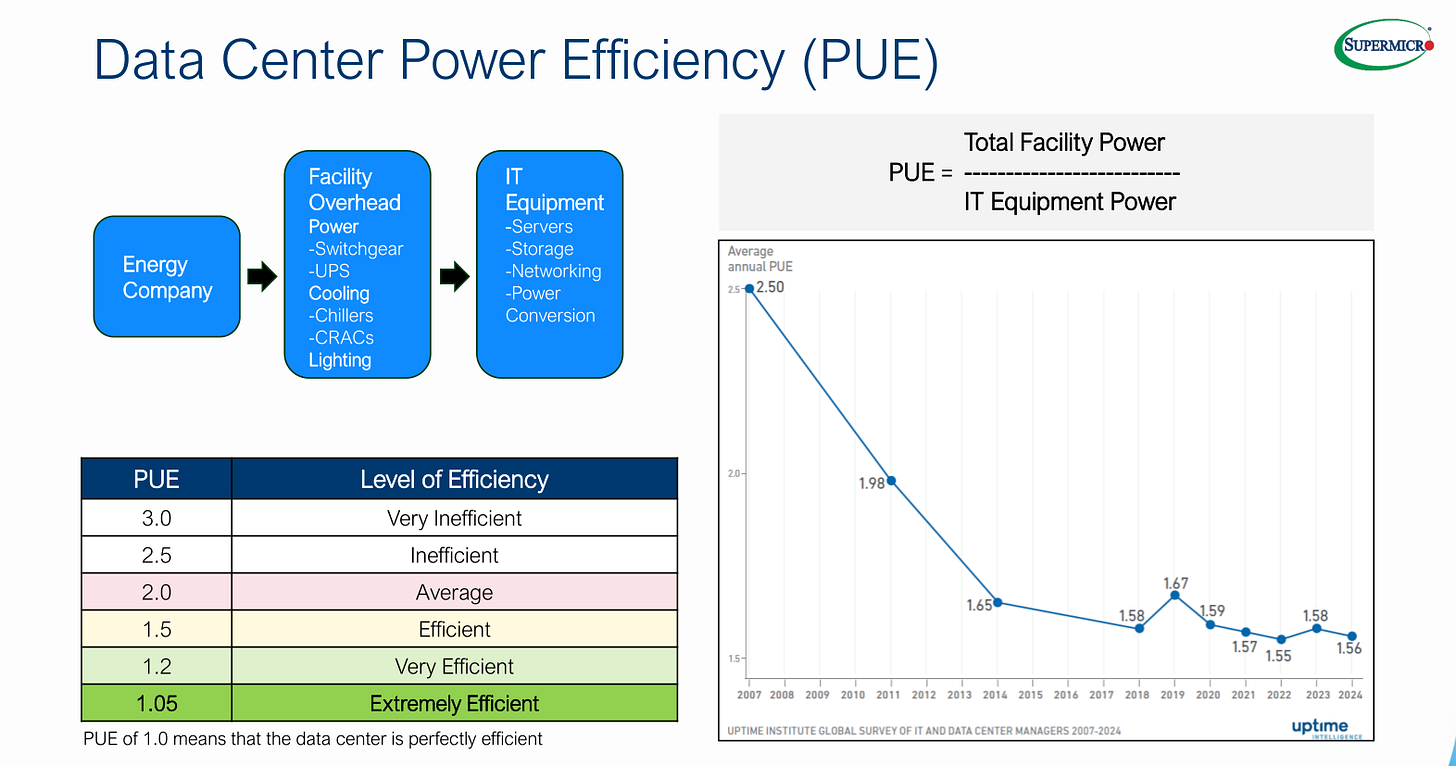
IIRC, the efficiency record is held by a Meta datacenter at a PUE of 1.02 but don’t quote me on that.
Wasting water to evaporation is a sustainability problem. Credit to the presenter for bringing this up and not dodging the topic.
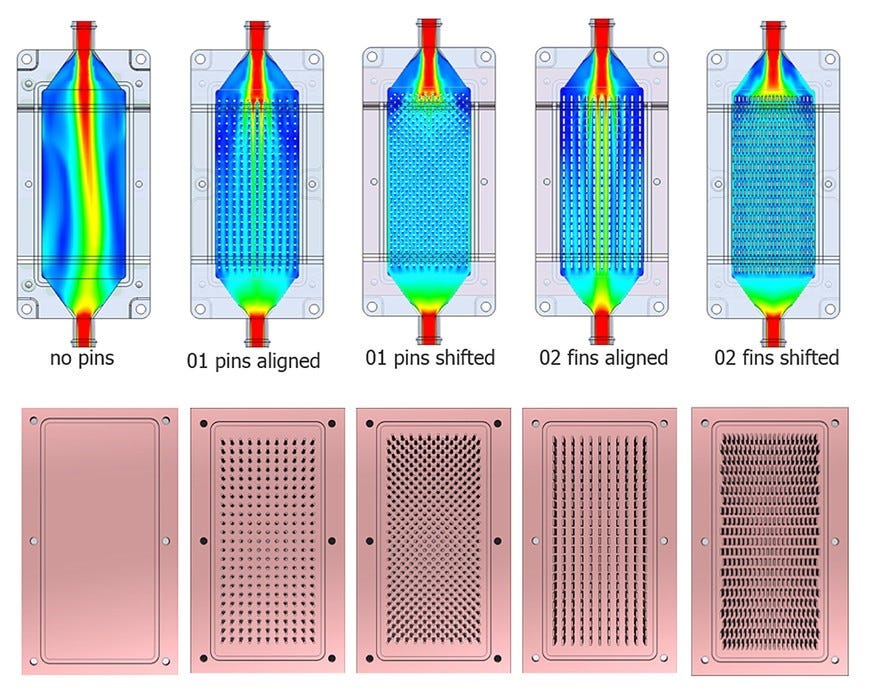
Cold plate design is a fun topic that was unfortunately not discussed in depth.
Fin shape, size, positioning, count, and offset are all important variables.
Direct liquid cooling has a massive advantage because high-powered fans in traditional air-cooling systems burn a lot of power. A 2U server that draws 2KW from compute can easily have 200W+ burned just from the fans.
A major limitation of direct liquid cooling is erosion. Fluid flow-rate cannot just arbitrarily go up. The cold plate micro-fins will erode, destroying thermal dissipation.
In Q&A, the topic of future scaling came up. Phase-change cooling (pressurized liquid go in, gas go out) was brought up and it seems to be the path forward.
A large amount of energy (heat) is dissipated from phase changes. There are obvious problems with the fluid composition as most liquid cooling loops use a mixture of 60% water, 40% glycol compounds, and minor quantity of anti-microbial and anti-corrosive additives. Each of these fluids have their own boiling points.
Nvidia is working on it though. “Two-phase” is the keyword.
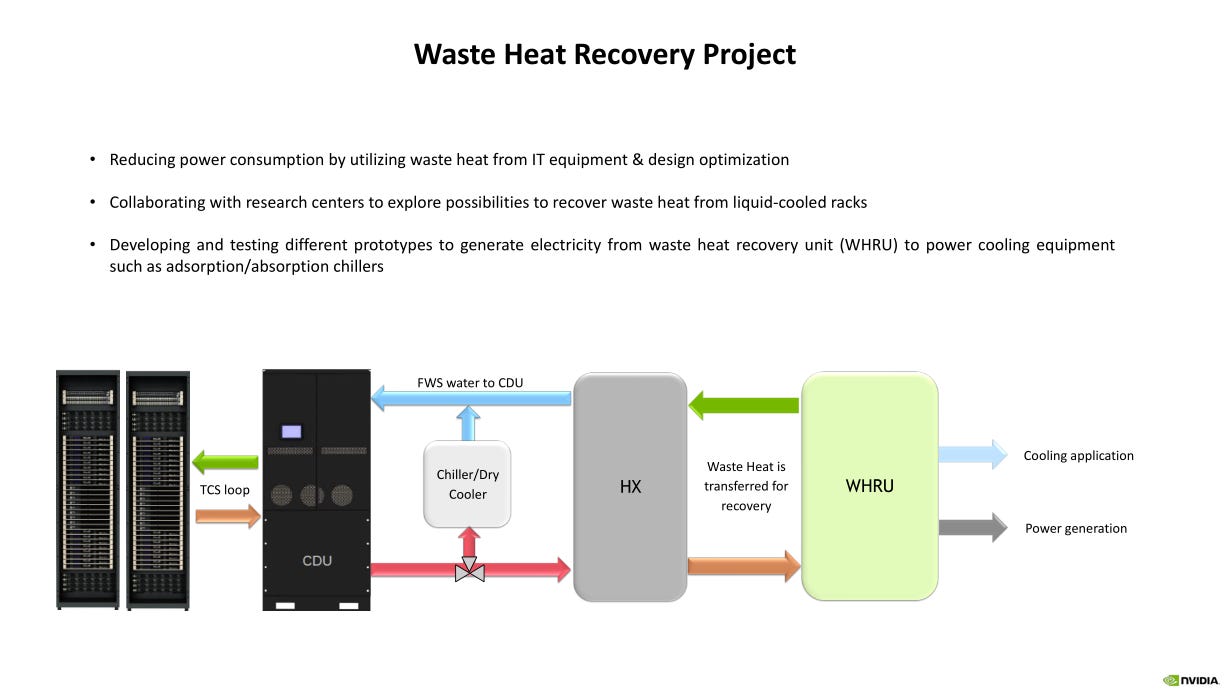
One neat idea shared is a waste-heat recycling project. Use warm fluid from a datacenter to heat up a neighboring agricultural facility such as a greenhouse or hydroponic farm. Waste heat electricity generation is also a possibility but seems much more difficult.
[2.e] Poster: Radix-8 FFT Accelerator
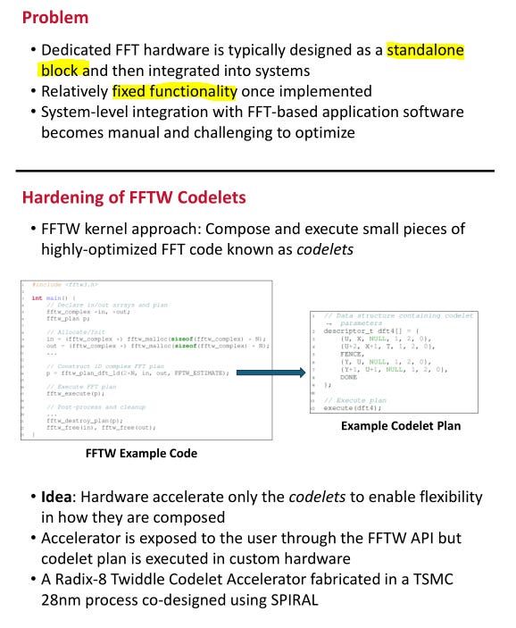
Here is the full poster. I will walk you through it in chunks.
Optimizing assembly code for FFT engines is difficult…
…because the engine is standalone. FFT operations are often mixed with other companion operations such as circular shift, windowing, and spectral density processing. The designers chose to create a codelet intermediate representation and optimize the hardware to that.
Essentially there is a flexible 8-point FFT engine paired with some complex multipliers that can be configured according to codelet instructions.
Neat poster.
[3] Meh
“Meh” presentations are somewhat interesting but are not compelling from a commercial perspective.
[3.a] Intel Lunar Lake
All the major chiplets on Lunar Lake are on TSMC N3B. Only the passive interposer is on an Intel process node. This product is great, but COGS is up 80-100%. This laptop chip is SO MUCH MORE expensive to manufacture compared to its predecessor, Metero Lake.
Lunar Lake might bankrupt Intel. Not joking.
Sell-side is modeling gross-margins going UP sequentially. This assumption makes no sense and is very wrong!
I will cover the recent INTC 0.00%↑ news, from board member resignations to activist defense prep to possible “strategic actions” next week. Subscribe so you get a notification/email as soon as it goes live.
With that pre-amble out of the way, let’s go over the presentation itself.
Nvidia applies their 70-80% gross-margin to on-package (HBM) memory. Intel’s CFO explicitly stated that they would be applying 0% margin on the on-package LPDDR5x in last quarter’s earnings call.
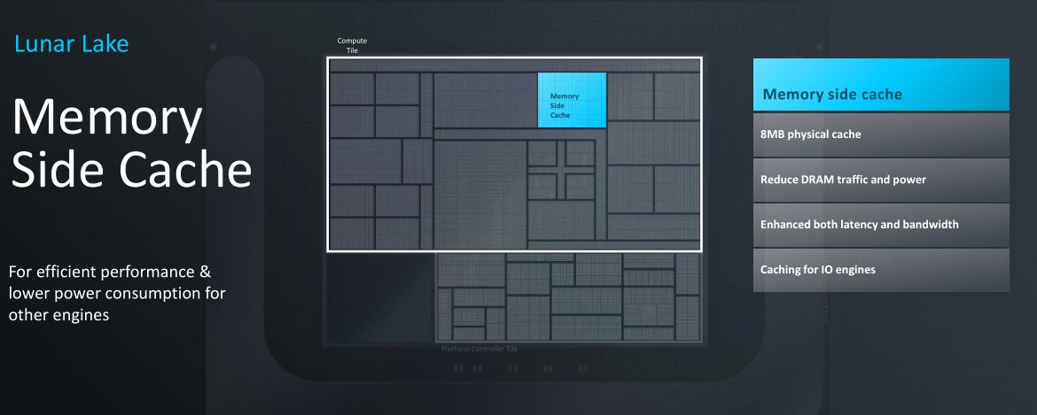
Memory side cache is analogous to the system-level cache (SLC) that smartphone SoC vendors have been using for years. Interesting that Intel chose to adopt this strategy for the first time. Perhaps it is to help the NPU and GPU not choke on the LPDDR5x bus.
E-core cluster gets its own power-delivery. They even made custom PMICs to support many separate power rails. Perhaps I was too critical of the Qualcomm PMIC situation. Nah. Qualcomm should have designed a new PMIC like Intel, instead of re-using PMICs designed for mobile chipset power levels (<5W) on a 55W part, running way outside of the efficiency zone and placing a comical number of PMICs in parallel and paying a hefty apology subsidy to laptop OEMs.
Anyway, back to Intel. The ML-based power management was vigorously roasted in Slack Q&A. These “ML models” don’t run on the NPU, obviously, because that would burn a ton of power spinning up the NPU…
Write this off as a marketing snafu. It’s fine.
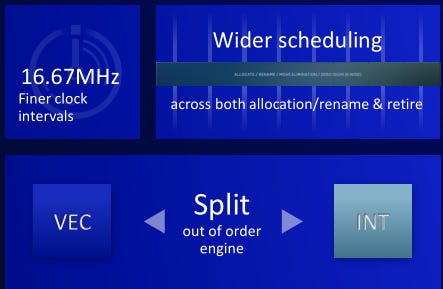
The P-cores have much finer clock scheduling. Traditional Intel cores only have granularity in 100MHz steps. Very interesting development. Probably helps with idle and light-use power consumption. Splitting the out-of-order engine for vector and integer is also interesting. Sacrifices area but likely gives a meaningful performance boost.
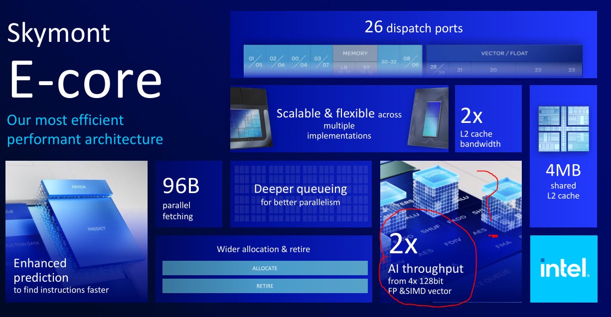
Who is running VNNI/vector workloads on E-cores? This seems like a waste of area.
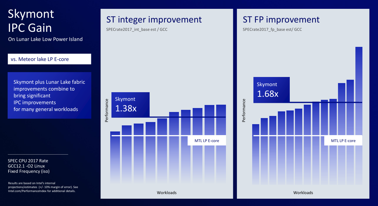
Integer performance boost of 1.38x gen-on-gen is great.
Power-efficiency is much more important, and they crushed it. Excellent job to the entire Skymont team! Looking forward to the server variant, Clearwater Forest.
Awesome latency improvements. The Windows scheduler should have a much easier time spreading applications across P and E cores.
Great data visualization. I hope my employer gives me a laptop refresh to Lunar Lake as the battery life of my 12th-gen, Alder Lake unit sucks.
[3.b] Intel Edge Xeon
These Xeon products are intended for edge operation, typically Telco, security systems, traffic systems, …
Lots of goodies are now integrated on-package, greatly improving throughput and power efficiency. Full CXL 2.0 support. Awesome.
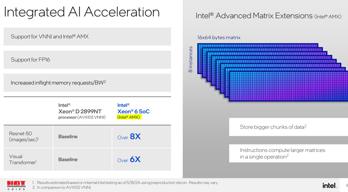
AMX is very useful for CPU-based AI. It is a real workload believe it or not.
A bunch of Intel proprietary accelerators are on the IO chiplet. The ones I highlighted are actually useful and broadly utilized by customers. Intel is… not in a good place right now so customers are not excited to write code to use most of these proprietary accelerators.
[3.c] Enfabrica
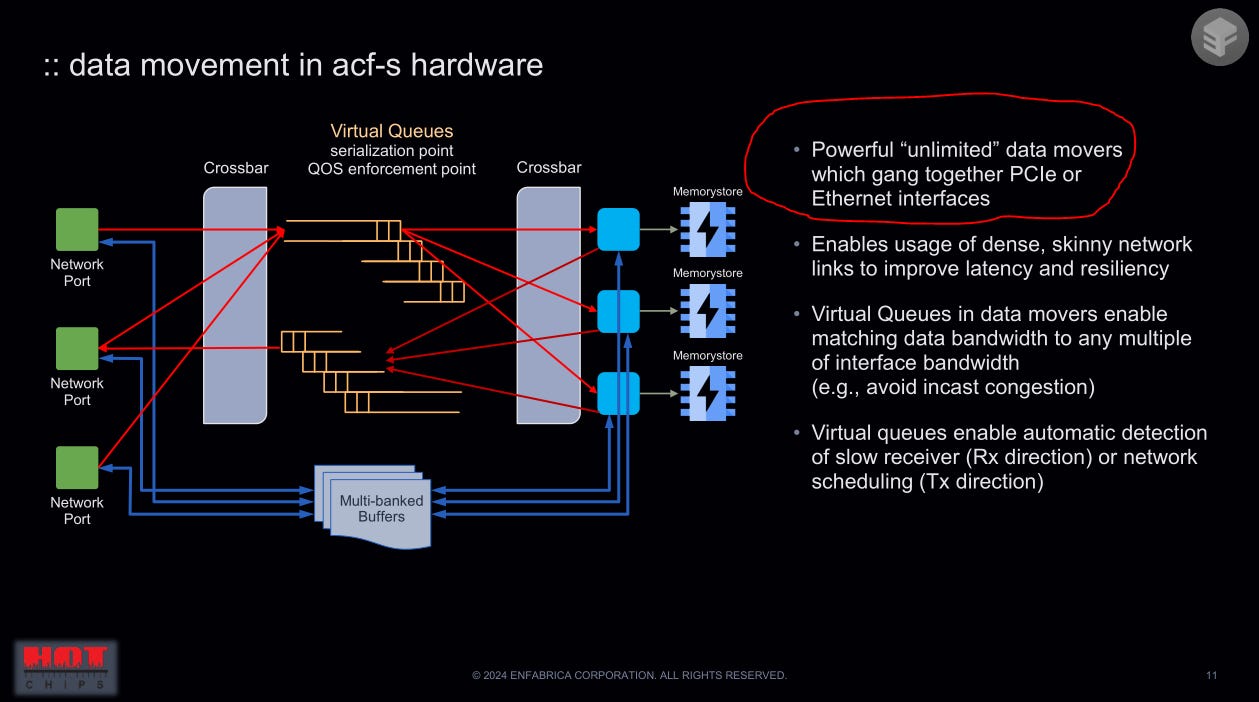
Weird, self-proclaimed “super-NIC”. Not sure why this chip exists or who would want to buy it… but it is super cool so worth covering.
If you don’t understand these slides… that’s ok. I don’t either. Only makes sense once we take a look at the chip block diagram.
Ok so this chip is a bizzarro, hybrid Ethernet + PCIe switch. Highly programmable, fully buffered, and extremely configurable from a radix perspective.
Again, not sure who would want to buy this, but it is very cool lol.
Great… burst absorption… but uh… wont the latency suck?
[3.d] Intel Silicon Photonics
This presentation was good but the AVGO 0.00%↑ one on the exact same topic was much better. Broadcom will commercialize their silicon photonics solution in 2025/2026 at high-volume while the team behind this Intel project is at high risk of getting cut in the impending layoffs. Really unfortunate. Wish the best for them.
No RDL layer. Probably results in better power efficiency compared to the Broadcom method at the cost of packaging complexity, and thus yield.
The lasers are on the photonic IC (PIC). Broadcom went out of their way to move the lasers off-die to external pluggable modules for serviceability and reliability.
Intel claims that their solution is reliable from field data testing.
Resolution of the plot is not great… but sure it looks like their reliability claims can be taken at face value. The presenter did not say how they accomplished this other than highlighting the quality of their photonic process node.
[3.e] SambaNova
Sambanova was my most anticipated presentation and… it was fine. The architecture is a CGRA, which is something in-between an FPGA and an ASIC.
Let’s unpack that.
ASIC is just a purpose-built chip that can be programmed with software but has rigid hardware features.
An FPGA is highly programmable using truth-tables (LUTs).
Imagine if you could create any chip design and flash it in under 90-seconds instead of spending $20-100M on tape-out and waiting 3-6 months for the chip to be printed. This is what an FPGA enables, at the cost of horrendous PPA.
CGRAs are somewhere in-between. A rare anomaly of computer architecture.
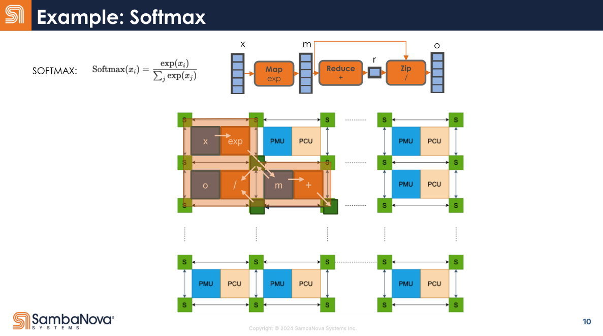
The ‘P’ in PCU and PMU stands for ‘pattern’. Idea of this architecture is to identify patterns in the workload, map them to weird, configurable SIMD things, and link them up in a uniform mesh switch grid. Sort of like the MUX trees of an FPGA.
Compute can be configured as a systolic array or SIMD vector unit; the former uses the broadcast buffer and the latter does not.
Remember friends, when you hear “programmer managed scratchpad”, think “pain, suffering, high skill-ceiling, and impossible compiler complexity”.
SambaNova decided to one-up Meta and make three separate mesh interconnects for their chip. Physical design and routing must have been particularly challenging… so congratulations to the engineers to pulled this off.
A mesh-ring hybrid top-level interconnect. Graph compiler team must have so much fun trying to make this work.
The main draw of this architecture is how it maps complex compute operations directly to the highly configurable hardware, enabling lots of neat optimizations.
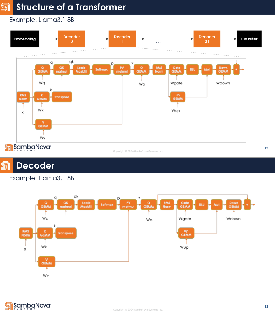
Here is a more complicated example:
They straight-up map this entire complicated transformer block directly to the hardware. Data just flows thru…
Lots of op fusion… opportunities.
Which lets them collapse kernel launch overhead (pink) and compute (dark green) very efficiently.
I am a big fan of how batshit insane this chip is. Want to believe it can be a real player in low-latency, high-throughput inference.
The engineers who attended claim that it only took a few hours to get Llama 3.1 working on the chip. They claim the compiler is good.
Wish them all the best. Out of all the AI hardware startups, SambaNova is my favorite but frankly, Nvidia and vertically integrated custom silicon will be very difficult to compete with.
[3.f] FuriosaAI RNGD
Why does this company exist?
To sell export-control compliant AI chips to China. Comparing yourself Nvidia L40S and Intel Gaudi 2 gives away your target market pretty decisivly.
This slide is why I bothered to cover them. Really awesome signal integrity and power integrity plots. Beautifull stuff.
[3.g] Frore AirJet
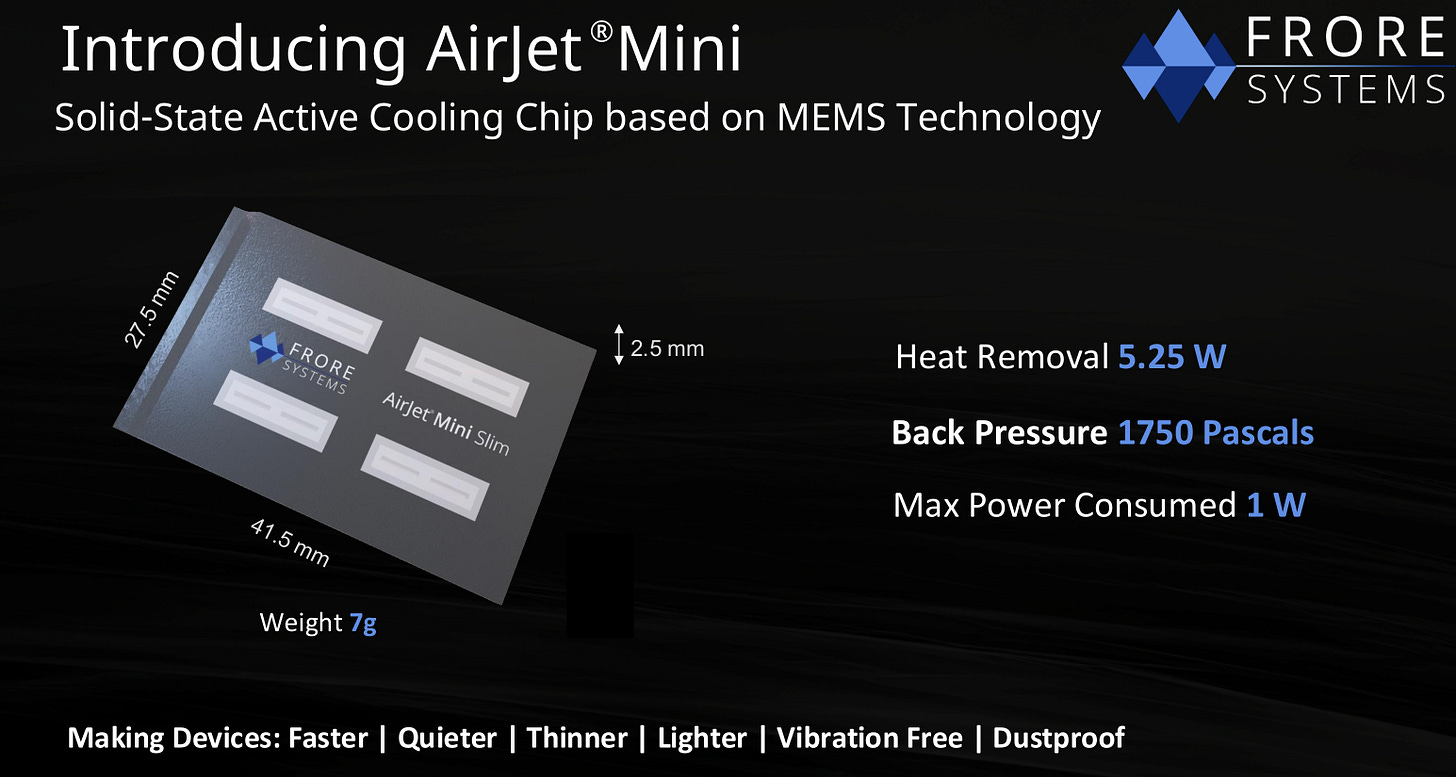
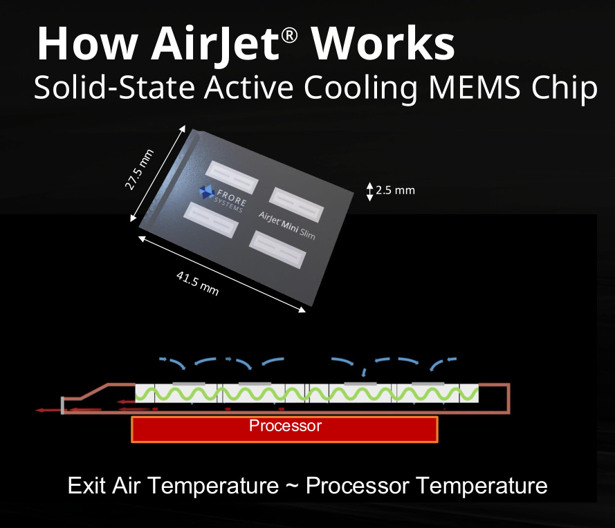
A solid-state, active cooling, MEMS chip. Super cool (pun intended). Very narrow market where they can sell this thing. Embedded IoT where thermal stability is important?
The MEMS vibrate in such a way that air is pushed out of the hollow inside of the chip. Allegedly, the vibrations are at a frequency that is not audible to humans. Dogs maybe, lol?
They have a custom non-silicon Fab which is interesting… not sure how they are paying for this given the limited commercial applications of the product.
All of these applications have strict battery limits. Burning 1W for active cooling seems like a terrible design tradeoff.
AirJet makes a lot of sense for embedded and industrial applications where any moving parts are a liability. Both of these use-cases have DC power inputs so burning 1W on active cooling is fine.
[4] Bad
This section is dedicated to two types of presentations:
Unviable products.
Delivery/content was so bad that attendees learned almost nothing new on excellent products/engineering.
[4.a] Tenstorrent
I am a Jim Keller fanboi but this presentation… did not inspire confidence in Tenstorrent’s future.
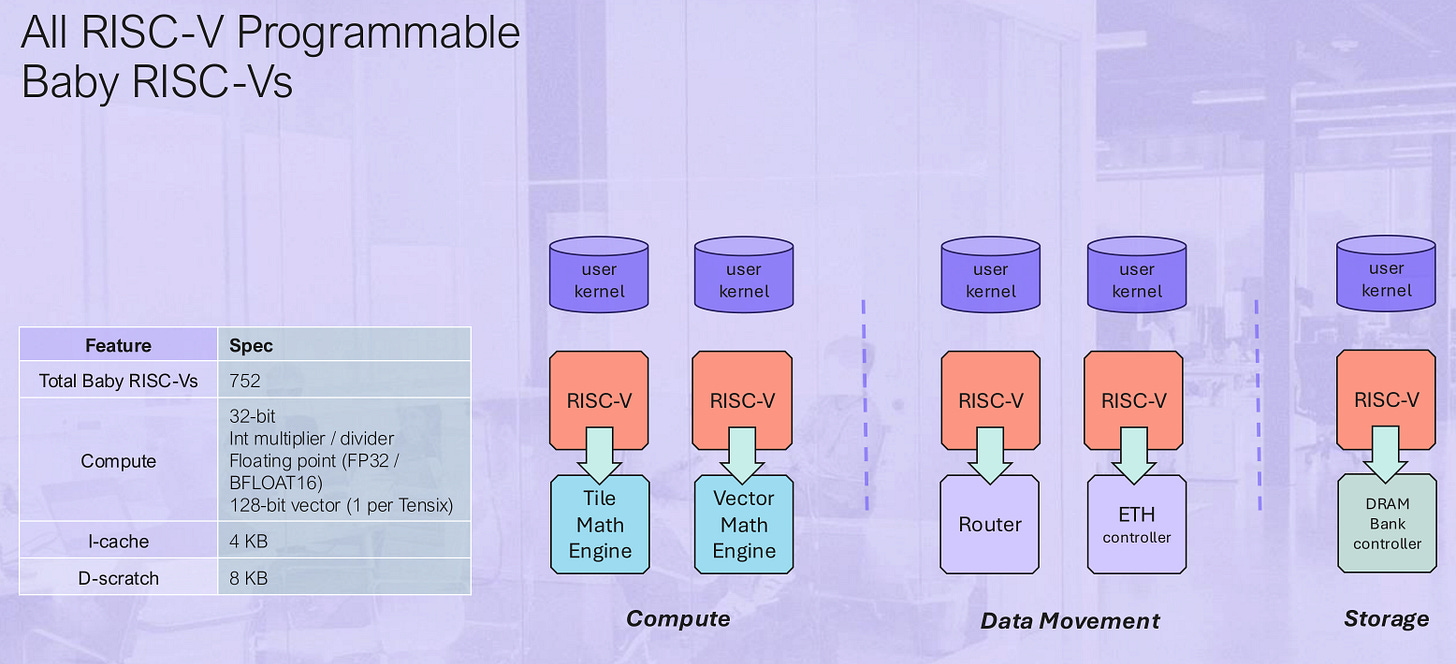
This architecture is “RSIC-V” to the max. Literally everything is controlled and managed by a baby RISC-V (super tiny) CPU core. Even DRAM and Ethernet control.
The compute cores have five baby RISC-V cores calling the shots.
Some mapping of neural network structures to the hardware is possible but not nearly to the degree of flexibility as SambaNova.
Here is a very important fact that was revealed in Q&A:
The baby RISC-V cores are heterogeneous depending on which higher level core they reside in. Each has it’s own ISA extensions.
RISC-V toolchain was already lacking and now Tenstorrent has multiple flavors and custom ISA extensions sprinkled throughout one chip. Compiler and programmer nightmare.
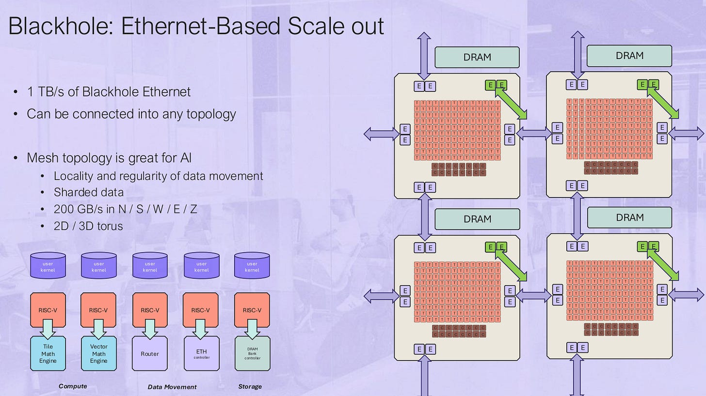
From a high-level, their scaling system seems elegant at first. Once core is one chip is one system. The programming model just extends outward to bigger and bigger systems because everything is Ethernet.
Latency non-uniformity almost certainly kills their chances with inference.
I spoke with someone (not Tenstorrent employee) at the conference and he said this TT-Metalium software stack is their 6th attempt. Credit to Tenstorrent for realizing the first five attempts were unsalvageable and starting from scratch.
They are way behind on the software front and the current (6th iteration) software stack delivers… not great performance. Thankfully, Tenstorrent is selling developer kits, and the open-source freaks are working hard on propping them up. They have a path forward, only because of the excellent, developer-first mindset.
[4.b] Nvidia Blackwell Advertisement Re-Run
Almost nothing in this presentation was new. Only the Quazar (brand name for OCP MX micro-scaling) stuff was new and worth covering.
Fine granularity quantization of individual rows.
Speedup depends on compute utilization and how the workload response to micro-scaling so take this table with a large crystal of salt.
Ah yes, the moat just got 10 feet deeper. Nice.
In Q&A, Dr. Ian Cutress absolutely roasted Nvidia, repeatedly asking if the Bluefield product line was dead. There is no BF4 on the roadmap. It is dead. The presenters sort of panicked and kept pointing to BF3 being on this slide. Very funny exchange.
[4.c] Literally Every Single AMD Presentation
AMD showed up to this conference determined to not share any new information and bore the audience into a coma. The content was bad. The presenters read from notes in the most boring, monotone manner possible, and nobody learned anything new.
There are only two slides I want to include, both from Victor (retired) Peng’s presentation.
Years from now when this bubble pops and we are all in economic ruin, the symbol of said bubble will be a fucking llama wearing blue sunglasses. Why are the sunglasses always blue? An anthropologist needs to answer this critical question.
One of the AI applications he highlighted is using AI to identify if fish are healthy.
HEDGE FUND, INVESTMENT BANKING, AND FINANCE SUBSCRIBERS, WE HAVE FOUND THE MISSING AI REVENUE. BUBBLE NO MORE.
Jokes aside, this is a real edge AI use-case.
[4.d] Cerebras Inference Pipedreams
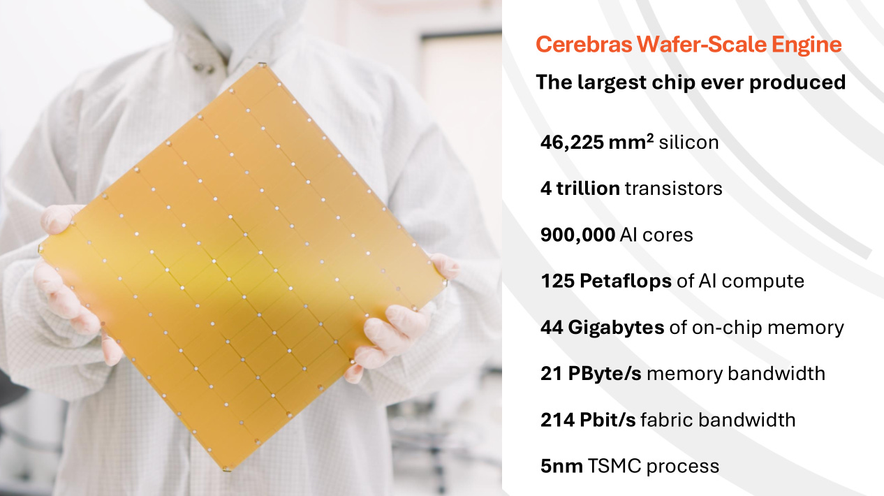
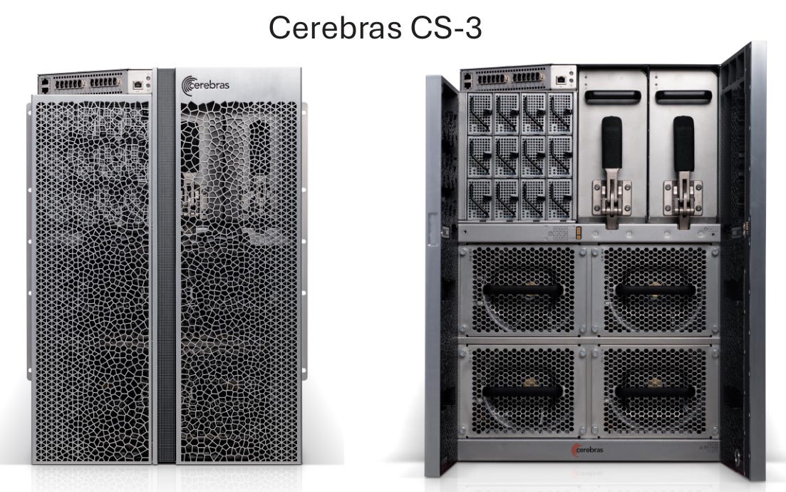
Cerebras makes chips the size of a wafer. They have developed incredible, breakthrough technologies to enable this.
Cross-reticle die stitching.
Cooling an entire wafer that burns like 20 KW at peak.
Power delivery.
PVT auto-management in firmware for stable clocks and high yield.
I am a huge fan of this company but will still mercilessly attack the false narratives they are pushing with respect to their AI capabilities.
This is an amazing HPC company. Biopharma, oil/gas, supercomputing, thermo/fluid simulations, nuclear simulations, bleeding edge science.
You have 44GB of SRAM on one chip. I would hope the performance of a tiny 8B parameter model is much higher than this.
The bandwidth and power efficiency is great… as long as you stay on one Wafer Scale Engine.
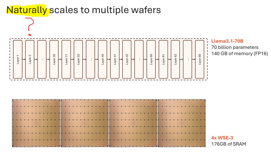
Llama3.1-70B is too large to fit.
Naturally? You hit massive latency problems because of the proprietary parallel-port, memI/O style interconnect for moving data from the wafer to Ethernet.
There are no Llama3.1-405B results in the presentation because they suck. This solution is not scalable. Cerebras managed to cobble together a few toy demos with small models and don’t have anything commercially viable.
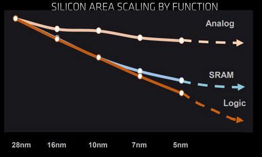
SRAM area scaling is super dead. When Cerebras moves from N5 to N3P, they will get effectively zero scaling SRAM, only logic. There is a one-time innovation possible in which they slap an SRAM-only wafer on top with hybrid bonding.
There are several factors that conflict with each other when trying to estimate the effective SRAM scaling of such a system.
Both wafers need significant area dedicated to TSVs.
The logic/normal wafer might be thermally limited.
Minor latency penalty for communication hits to the SRAM wafer.
I have no idea what the area ratio is for SRAM/logic on the existing WSE because none of the diagrams are to scale and the wafer images are too uniform.
Let’s be generous and say a next-generation WSE with a hybrid-bonded SRAM wafer will achieve 1.8x SRAM capacity scaling. After that, it’s over.
Cerebras loves to talk about a “GPU/HBM wall” but they have a wall too, a SRAM wall.
[4.e] Microsoft Maia
Frankly, this presentation was just bad. Out of all the hypsercalers working on custom AI accelerators, Microsoft is dead last. The only nice thing I have to say is at least the Maia team showed up and presented, unlike Amazon Trainium/Inferentia.
Two generations of HBM behind… and why is provisioned TDP 200W lower than designed TDP? Did they realize the performance is so bad that underclocking is the only way to salvage the project?
No performance data. Generic information. They don’t have anything.
[4.f] Intel Gaudi 3 (is already dead)
The Gaudi products are from an acquisition Intel made back in 2019, Habana Labs. As is tradition, Intel mis-managed the acquired company into oblivion and has discontinued their products.
Gaudi 3 is the last Gaudi. The next product is a GPU called Falcon Shores that will use the OneAPI software framework. None of the Gaudi chips support OneAPI. Falcon Shores will not support the Gaudi software stack. Zero forward compatibility.
VLIW compute units. None of the software stack is gona make it into OneAPI or Falcon Shores.
[4.g] Tutorial: Qualcomm On-Device AI
This presentation was a copeium advertisement for QCOM 0.00%↑ irrelevance in the genAI era.

Sub-10B LLMs suck. Why have a bad experience when a much better experience is less than 150ms latency away in the cloud?
LLM models also burn through all the user’s battery when run on a smartphone, turning the device into a hand warmer. Why should anyone generate images locally on their phone when much higher quality images can be generated in the cloud using industry-leading wireless connectivity?
I bought one of these Snapdragon X Elite laptops and struggled to get the NPU to activate at all. After hours of trying, I found one workload that only activated the NPU to 3% utilization according to task manager.
[4.h] Phononic Solid-State Cooling
Here is another solid-state cooling solution but with an utterly implausible commercial pitch. This device was designed to control the temperature of optical engines and other highly sensitive loads. Use a lot of power to make sure the target device stays in a narrow temperature band.
They have made a product that has no reason to exist. A tower air cooler that can have solid-state active cooling kick-in to dynamically increase thermal dissipation.
Why is this better than just spinning the fans at a higher RPM?
Does the efficiency of this system make sense? (No!)
[5] Dumpster Fire
No redeeming qualities.
[5.a] Ampere Computing
Ampere Computing is a company that made a niche product, cloud-optimized ARM (ISA) CPUs, and has since been abandoned by every single customer they had except ORCL 0.00%↑ who only buys chips from Ampere Computing because they have massive bags.

<COUGH COUGH> RELATED-PARTY ROUND-TRIPPED REVENUE <COUGH COUGH>
I will be adding some subtle enhancements to the slides. See if you can spot them.
There is a paradigm shift, to an army of competitors that do your niche better. Competitors who have real 3rd-party customers.
It’s not just the ARM semi-custom chips cloud hyperscalers have made. Intel and AMD both have compelling x86 products in this cloud-optimized market segment. Intel Clearwater Forrest looks incredible.
There are rumors that the mesh is licensed from ARM. Last generation, they had a custom mesh.
They compare perf/watt against Genoa (not the real competing product) when Bergamo data is literally on the same slide!
Let’s fix that.
Intel Clearwater Forest and AMD Turin dense (2025 release) will beat Ampere Computing to market and annihilate them in perf/watt.
Nobody is running these inference workloads on CPUs. The actual CPU inference workloads (tabular data, heavy financial inference) run on Intel Xeon because of the excellent AMX extensions, accompanying software stack, and broad x86 ecosystem.
Indeed, the ecosystem is ready. All your customers (excluding Oracle) bought your chips to port their software to ARM and have now gone vertical.
[5.b] SK Hynix In-Memory Compute
Every in-memory compute project has the same problem. The process node for memory is very bad if you try to add logic. PPA of complex transistor structures is really bad on a process designed for highly uniform capacitor banks.
This SK presentation did not address any of this process tech stuff.
To evaluate these compute-in-memory GDDR6 chips, they needed a FPGA host, purely for testing.
Except none of the test results are real. It’s all simulations as the prototype they are presenting has not been brought up yet.
In Q&A, they were absolutely roasted. It was argued that spending R&D effort on reducing the energy cost of memory interfaces to main logic would be far more productive than trying to fuse compute into the memory die itself.
This idea does not work (no test data) and has no commercial future.
[6] Terrifying — Trevor Cai, the OpenAI Guy
This presentation is so special, it deserves its own category.
[6.a] Excellent Technical Material
Silent data corruption (SDC) is a problem that got a lot of attention. I wonder if the source of these SDCs is GPU SRAM or logic/timing faults.
Wonder if he thinks the new Blackwell RAS engine is enough. What gaps are still there in self-test coverage.
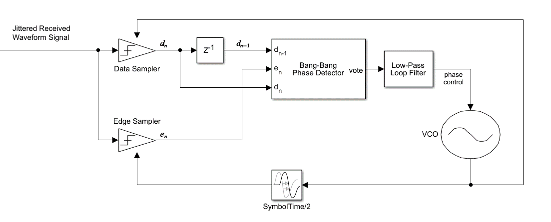
Link-flaps on one port effecting neighboring network ports is very difficult to mitigate. Bad links effectively behave like sinusoidal noise sources, dumping jitter/noise into neighbors. The SerDes CDR needs to be more robust.

Induced noise from a degraded link depends on the CDR design. The commonality is an oscillator dumping asynchronous noise via electromagnetic coupling and/or supply/ground pollution.
Interesting that transient power response is becoming problematic for cluster stability.
OOB power management is possible by using firmware and board-level PMICs, shunt resistors, ADCs, and so on.
Making that OOB power telemetry both accurate and low latency is uh… extremely difficult. Manufacturing variances in silicon, PCB material, and analog surface-mount components make current measurements surprisingly inaccurate. Synchronizing thousands of I2C-triggered measurements is a challenge by itself, to say nothing of the latency issues.
Wonder what the latency requirement would be. 10 ms? 200 ms?
[6.b] “Sometimes lines really do go up”
We can curve-fit observations to predict future scaling!
But actually no. Scaling went from 6.7x to 4.2x per year.
So… which is it? Can we arbitrarily curve-fit empirical data and extrapolate to infinity or not?
Trevor Cai, the OpenAI guy, tried to make an economic argument that I strongly disagree with.
“Sometimes lines really do go up.”
Both of the examples he gave have decisive counterarguments.
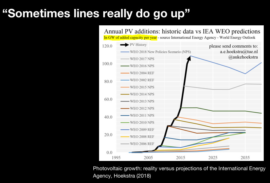
[6.b.i] Solar Panels
Oh, wow the International Energy Agency repeatedly mis-predicted solar-power capacity expansion trends. Well… they did not predict China state-run economic policy encouraging massive un-economic capacity expansions and dumping solar panels below COGS!

Ironically, this example of why we should not be worried about a massive genAI bubble demonstrates why we would be terrified!
What happens if all these datacenters produce nothing more than 10 duplicative chatbots of similar performance with no meaningful demand?
Massive. Compute. Overcapacity.
[6.b.ii] Moore’s Law
Funny how Moore’s law is brough up as a defense for lines go up.
Moore’s law has always been an economic law. It makes sense to move to a new, denser process node because the economic value of the product goes up.
Huge up-front CapEx spend for Fabs is justified because the demand will be there for the latest node.
Except this has changed. The latest nodes are too expensive.
Chiplets are being used as a cost-saving strategy. Everyone is trying to minimize content on 3nm-class nodes.
Some products that would traditionally be launched on the latest node are instead choosing N-1.
Many products will not move past the 3nm-class (TSMC N3E/P/X, Samsung SF2, Intel 18A) generation. This era of process technology represents a cost wall.
Moore’s law is dead, not because transistor scaling is dead. Chiplets and advanced packaging will keep density scaling alive.
The economic facet of Moore’s law is dead.
It no longer makes sense to move every product to the latest node.
It’s over. Line no longer go up.
[6.c] Surreal Bubble Inflation
Sitting in the audience listening to this presentation was surreal. It was like watching a bubble inflate in real time.
Someone in Q&A asked about ROI. You know shit has gone off the rails when engineers are asking about ROI at a technical conference.
To demonstrate the absurdity of where we are, I have created a meme using one of my favorite films, “The Big Short (2015)”.
We are going so much higher. DotCom and tulips got nothing on genAI.
[7] Winners and Losers
Ok, investment time!
Here are the winners and losers (with runners up) divided amongst public and private companies.
Public Winner: AVGO 0.00%↑
The co-packaged optics presentation was incredible. High-quality test data shared with maximum confidence. Excellent technical details. Bravo.
Public Winner Runner-Up: NVDA 0.00%↑
Galaxy-brain researchers work at Nvidia, developing innovative AI-based chip design techniques that yield massive productivity boosts and performance improvements.
Private Winner: OpenAI
Thier chip-design and infrastructure team is kickass. Very excited to see what they put together in the coming years. They are going to raise a new funding round at $100-125B valuation and dump that money into making breakthrough chips.
Bubble is inflating but that is a problem for the future.
Private Winner Runner-Up: Cerebras
Many poorly informed investors are going to fall for the inference story Cerebras concocted. IPO will pop. Try to get allocation on the way up, then find an opportune moment to short them aggressively.
DO NOT SHORT THEM WITHIN THE FIRST MONTH OF TRADING.
Cerebras is a good company that makes a niche HPC solution. Quality engineering that deserves some valuation, just not an AI hype valuation.
I admire the incredible engineering Cerebras has and would love to own shares long-term once the bubble pops and they are appropriately valued as a breakthrough HPC company, rather than an AI head fake.
Public Loser: MRVL 0.00%↑
Broadcom is going to crush this company. CPO will destroy the oDSP business. The incredible new custom-silicon platform will poach Marvell customers over time.
To be clear, the short-term outlook for Marvell is amazing. Amazon orders, oDSP, and (hate to admit this) telco market recovery are all going to hit at once and make this ticker moon.
DO NOT INVEST IN THIS COMPANY LONG TERM.
PLAN TO BE OUT BY SUMMER 2025.
Public Loser Runner-up: INTC 0.00%↑
Lunar Lake is going to annihilate gross margins. Sell-side and the finance community have no idea what is coming.
Private Loser: Ampere Computing
They have no customers other than Oracle, who have heavily invested in them.
**The vast majority of revenue is related party revenue.**
If they ever make it to the public markets, I will short them in size and write a detailed short report in LaTeX.
Day one short. Long ARM 0.00%↑ for the most concentrated alpha trade of all time.
Private Loser Runner-Up: Tenstorrent
This architecture is too damn complicated. No human can hope to program this PHD science project that somehow has a $2B valuation.
Someday, Artificial Super-Intelligence (ASI) will be created on someone else’s chip and only ASI will be able to effectively program Tenstorrent architecture.
I have an earnings post coming late next week that includes NVDA 0.00%↑ MRVL 0.00%↑ AVGO 0.00%↑ a special INTC 0.00%↑ update, and an update on all my portfolio holdings. The spreadsheet I made years ago was never designed to keep track of short positions, hence the re-build from scratch and delay.
















































![[V]ery [L]ong [I]ncoherent [W]riteup](https://substackcdn.com/image/fetch/$s_!lVhT!,w_140,h_140,c_fill,f_auto,q_auto:good,fl_progressive:steep,g_auto/https%3A%2F%2Fsubstack-post-media.s3.amazonaws.com%2Fpublic%2Fimages%2F1335e244-45bb-4add-a677-d9ab1ed74702_875x957.png)


![[1/3] Dell XPS (TributoQC) 13 Review](https://substackcdn.com/image/fetch/$s_!xPDW!,w_140,h_140,c_fill,f_auto,q_auto:good,fl_progressive:steep,g_auto/https%3A%2F%2Fsubstack-post-media.s3.amazonaws.com%2Fpublic%2Fimages%2Fb4ecb4fc-5e71-46b2-995b-66adecffbac0_842x614.png)






Any ideas on why blue field might be canceled?
TY for the writeup!!