


High Bandwidth Flash and Sandisk Investor Day 2025
If it sounds like cope, it probably is cope.

Irrational Analysis is heavily invested in the semiconductor industry.
Please check the ‘about’ page for a list of active positions.
Positions will change over time and are regularly updated.
Opinions are authors own and do not represent past, present, and/or future employers.
All content published on this newsletter is based on public information and independent research conducted since 2011.
This newsletter is not financial advice, and readers should always do their own research before investing in any security.
Feel free to contact me via email at: irrational_analysis@proton.me
I am short WDC 0.00%↑ because of NAND flash. Sandisk is the flash part of WDC that is about to be spun out. Probably will need to cover the Western Digital Short and re-short the new garbage.
Long MRDIMM, Short NAND Flash

Irrational Analysis is heavily invested in the semiconductor industry.
Today I want to briefly cover the recent Sandisk event and dive deeper into an obvious red herring bullshit technology: “High Bandwidth Flash”.
This is one of those situations where I know thing is bullshit but needed a little time to prove the initial gut feeling.


ONTO 0.00%↑ just reported earnings and says NAND CapEx going up. All of your competitors are continuing to participate in the layers race. Choosing to sit out of a competition does not mean the competition no longer exists. 🤡

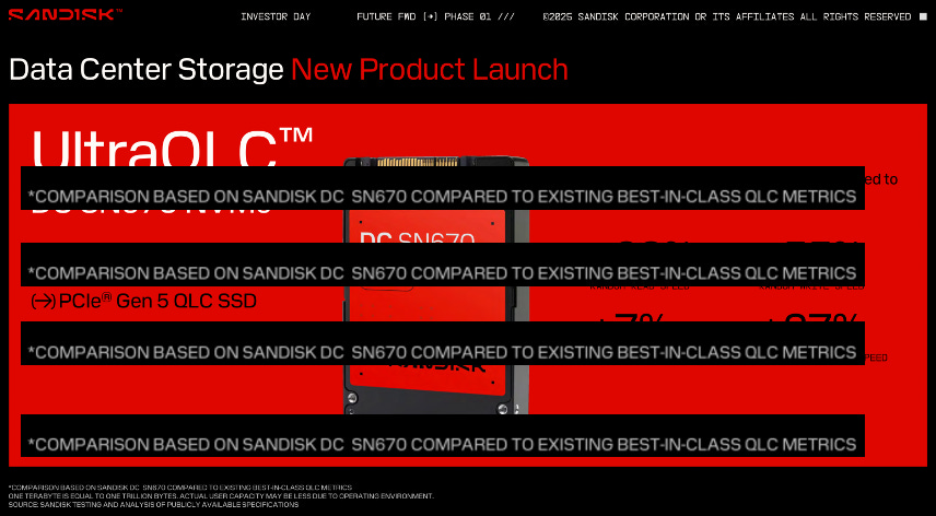
QLC without compromise? Got any details?

Looks like bullshit. Just like those Intel Lunar Lake “AI power management” claims from Hot Chips 2024.
Which product are you comparing against? The specifications are public. Shouldn’t the competing QLC product be named in the fine print?
Why not compare your own product with and without the fancy controller hardware accelerators enabled? That would give a good A/B comparison of the tech.

Our violently cyclical business is going to be stable going forward. You gotta beleiveeeeeeeeee!
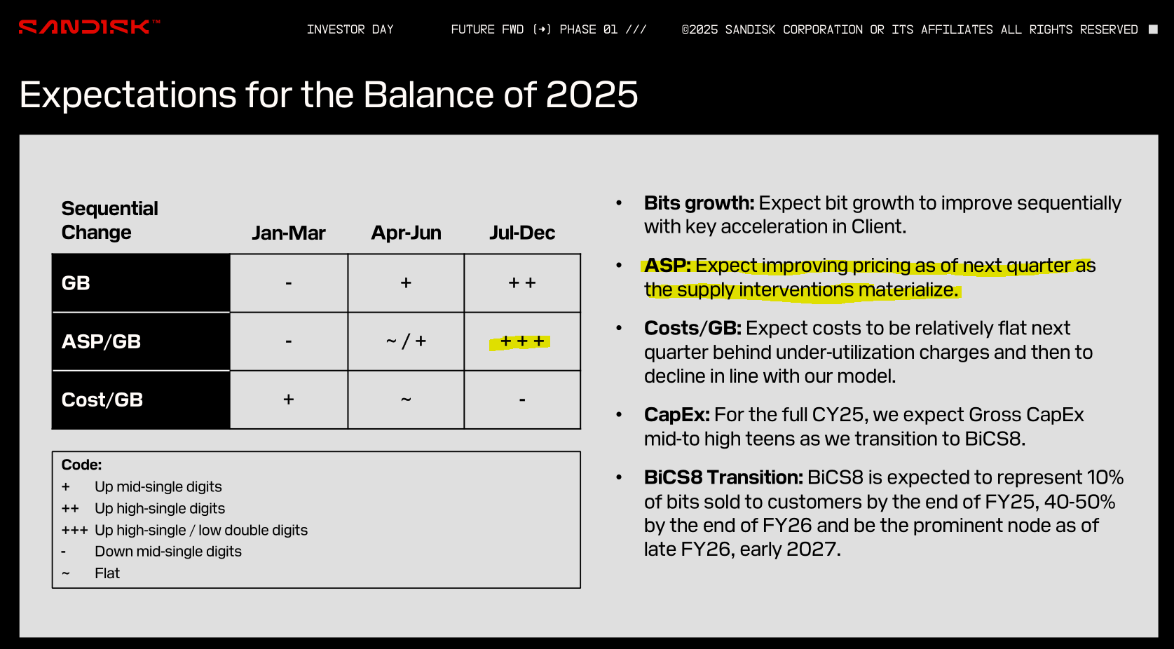
Supply interventions refer to Samsung and Micron both cutting NAND wafer starts.
YMTC is not cutting lol.
And now we get to the fun part. This is clearly too good to be true… but we must go deeper to prove it.

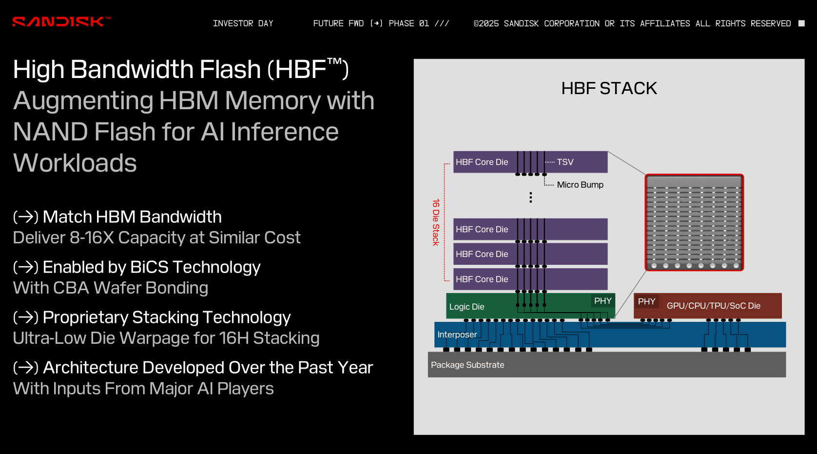
Same electrical interface? Only “minor” protocol changes?
That means there only needs to be minor changes to the controller/PMA. Why the need for a standards body? Just write some simple digital IP and open source it.
Something is not right…
My first thought is that Sandisk made zero mention of durability.

NAND flash has a write endurance. Controllers must track bad blocks and remove them from the mapping table. None of the slides presented by Sandisk indicate they have made architectural changes to the NAND cells to improve durability.
Given how aggressively AI researchers complain about silent data corruption (SDC), this seems like a nightmare. NAND flash wear out is a well-known reality. Every commercial product has over-provisioning. Extra “hidden” capacity that is used to replace worn out cells over the expected life of the device.
There is also the issue of read/write granularity.
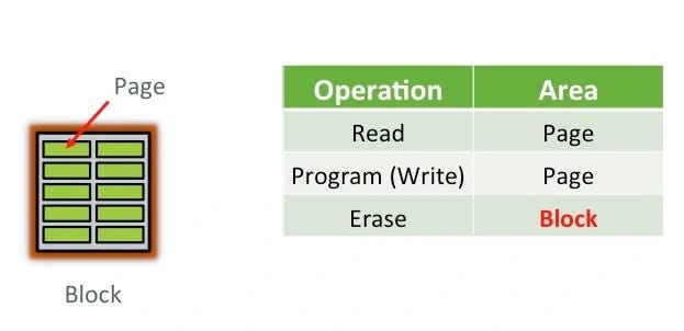
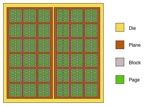
NAND flash is designed to be read and written at a page level.
Page size is usually 4-16 KB.
HBM3 is accessed in 32-byte packets.
Bytes. Not kilobytes.
I make have gotten the exact numbers wrong, but this is directionally correct.
Key Flaws in Sandisk High-Bandwidth Flash Concept:
NAND endurance will lead to horrible error rates and silent data corruption.
Reads and writes are in far larger chunks (less granular) when compared to HBM/DRAM.
Existing software is not written to handle this limitation.
The changes needed on the controller side are not “minor”… they are massive!
That is all for today. Brief note.

I have a very exciting optics project in progress. It’s going to be great.

Goal is to finish and publish by Sunday 2/16. Might need another weekend to finish it.
So, did SanDisk seriously try to position QLC flash NAND for critical data storage? Or did I misread that?
Unrelated to this, Intel had really cool tech for this kind of application - Optane. Unfortunately, they discontinued working on it a few years ago and shut it down - great timing 😜.
TYVM