
A Background-Proof Guide on Process Development Kits
A practical approach.

Irrational Analysis is heavily invested in the semiconductor industry.
Please check the ‘about’ page for a list of active positions.
Positions will change over time and are regularly updated.
Opinions are authors own and do not represent past, present, and/or future employers.
All content published on this newsletter is based on public information and independent research conducted since 2011.
This newsletter is not financial advice, and readers should always do their own research before investing in any security.
Feel free to contact me via email at: irrational_analysis@proton.me
Process Development Kits (PDKs) are perhaps the most poorly understood sub-section of semiconductors. It’s mostly because of all the secrecy.
Documents and data associated with PDKs are the most NDA-ed stuff out there. Very aggressive watermarking.
Today I want to help all of you understand what is actually in a PDK and why it matters. Lots of practical issues depend on these top-secret documents, statistical models, and library files.
My first public post is a high-level guide on the entire semiconductor lifecycle with a fake chip design walked through from start to finish.

Consider this a deep-dive into specific parts of semiconductor development.
Four textbooks were used to develop the material.
CMOS VLSI Design: A Circuits and Systems Perspective by Weste and Harris
Foundations of Analog and Digital Electronic Circuits by Agarwal and Lang
Principles of CMOS VLSI Design: A Systems Perspective by Weste and Eshaghian
Semiconductor Device Fundamentals by Pierret
For a full list of recommended books and resources, please refer here:

I have written this material with the goal that **anyone** can understand and learn something new. No pre-requisites and no dumbing-down either. If you only understand 20% of this post, that is still a huge win IMO.

Let’s get started.
Contents:
What is in a PDK?
Basic Theory
Ideal Basic Devices
Resistor, Capacitor, Inductor
MOSFET (Popular Transistor)
Stackup
Design Rules
Practical Issues
Device Parasitics
Wire Network Parasitics
Electromagnetic Coupling
Process Variation
Temperature Sensitivity
Voltage Uniformity
Electromigration
Leakage and Noise
Detailed Example: Capacitors
Design-Technology Co-Optimization (DTCO)
Derivative Nodes
Library Managment
Simulations: Garbage In? Garbage Out!
Bump-Out (Packaging)
Overview of the three leading-edge logic foundries.
[1] What is in a PDK?
A Process Development Kit (PDK) consists of three primary categories of materials.
Standard Cell Libraires
Transistors
Resistor, Inductor, Capacitor (RLC)
Higher Level Blocks
…
Models for the process, voltage, and temperature (PVT) sensitivity of devices.
Gain behavior
Noise
Parasitics
…
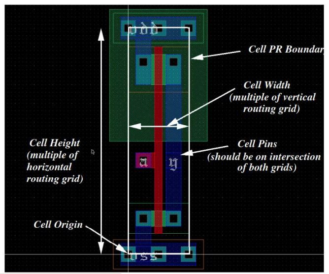
Thousands of slides and pages of documentation that provide guidelines on how to place cells, improve yield, mitigate parasitics, and so on.
Standard cells are like building blocks.

[2] Basic Theory
Digital signals do not exist in the real world. They are simply a very powerful abstraction.

Analog problems need to be accounted for. For example, the rise/fall time of a transistor (switching element).

Failure to do so results in bit errors, breaking the digital abstraction.
Chips are 3-dimentional structures. “Stick Diagrams” are a useful tool for visualizing what is going on.

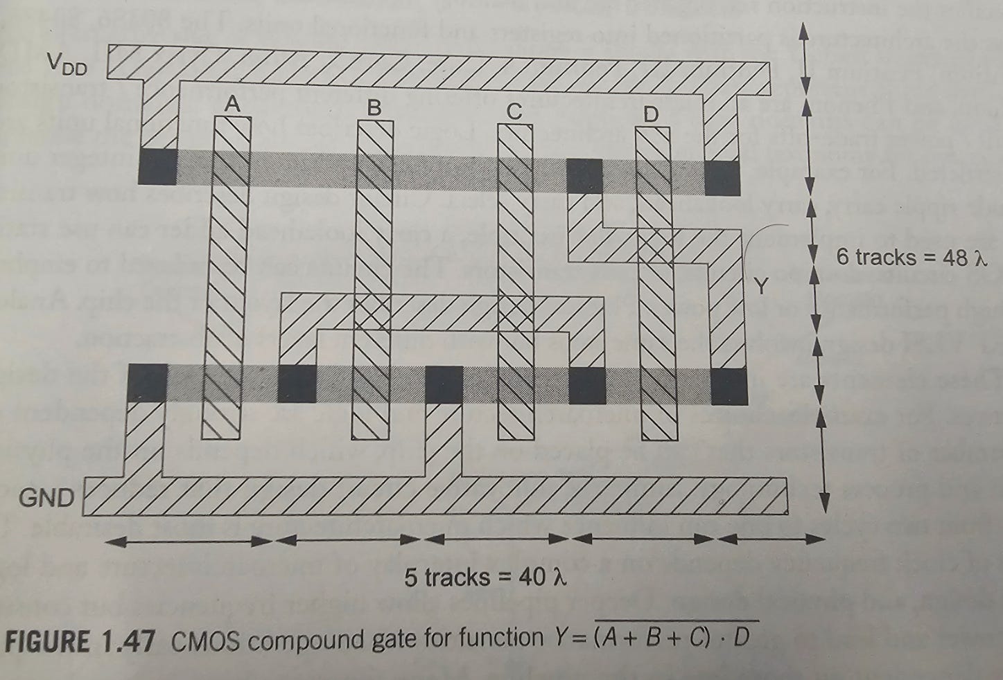


Think of these as top-down views of a structure.
PDKs have libraries full of variants of the same structure. Each version of the structure offers different tradeoffs.
For example, here are eight (8) versions of the same basic inverter.


Logic Foundries and design companies do not make up many versions of the same standard cell for fun. Various performance, area, and power characteristics drive the creation of so many “redundant” cells. (its not redundant)
Finally, the dynamic (frequency) response of a circuit is what really matters in most scenarios. To understand frequency response, we need to go beyond simple resistive models (V = IR). We need impedance.

Impedance is a circuits resistance to an AC (sinusoidal) input. This will hopefully make more sense shortly.
[3] Ideal Basic Devices
Note that everything in this section is ideal. Real devices do not behave like this!
[3.a] Resistor, Capacitor, Inductor
Resistors are obvious. They simply create a voltage drop.
Capacitors and inductors are energy-storage elements.
Capacitors (aka caps) are typically built with two parallel plates.
Inductors (aka chokes aka coils) are typically built with wire wounded in a circular manner.
Let’s look at the basic time-domain response of these energy storage elements.


Similar analysis for inductors…


Time-domain responses are of limited use. What we really need for proper analysis is the frequency response. In other words, the response of a circuit to a sinusoidal input of arbitrary frequency. Impedance.


[3.b] MOSFET (Popular Transistor)
There are multiple types of transistors. The Metal-Oxide-Semiconductor Field-Effect-Transistor is the most popular and important flavor.


The physics and complexities of material science are a topic for another day.
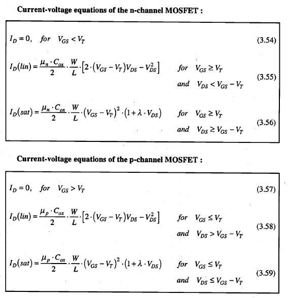
All you really need to know for this post is that transistors are voltage controlled switches.

And the math of an ideal MOSFET looks like this.

There is a separate curve for gate-source (“control”) voltage.
As the voltage across the switch (drain-source) increases, the current across the switch also increases… up to a saturation point.

Ideal MOSFETs are modeled with three regions. The math is a piecewise function.
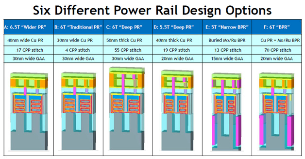
[4] Stackup

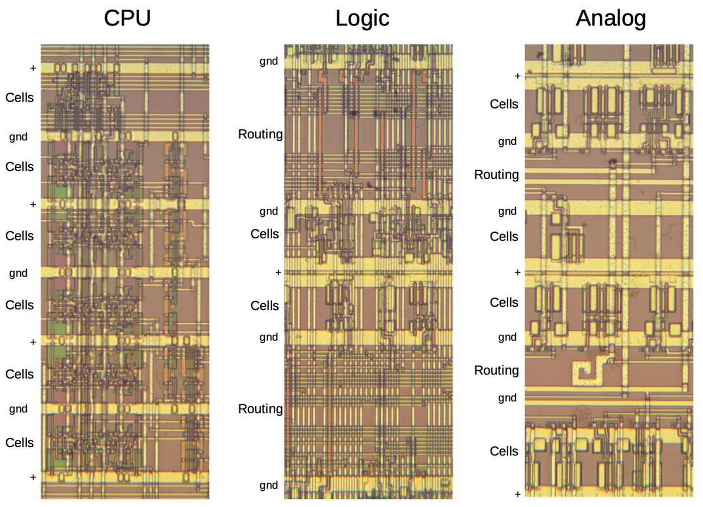
Every process node has multiple “stackup” options. How many layers (and of what thickness) are available for designers and automated tools to use.
In general, the transistors are at the bottom and the wires are above. This is over-simplified. Various analog components can be on many different layers.


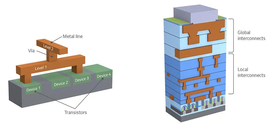
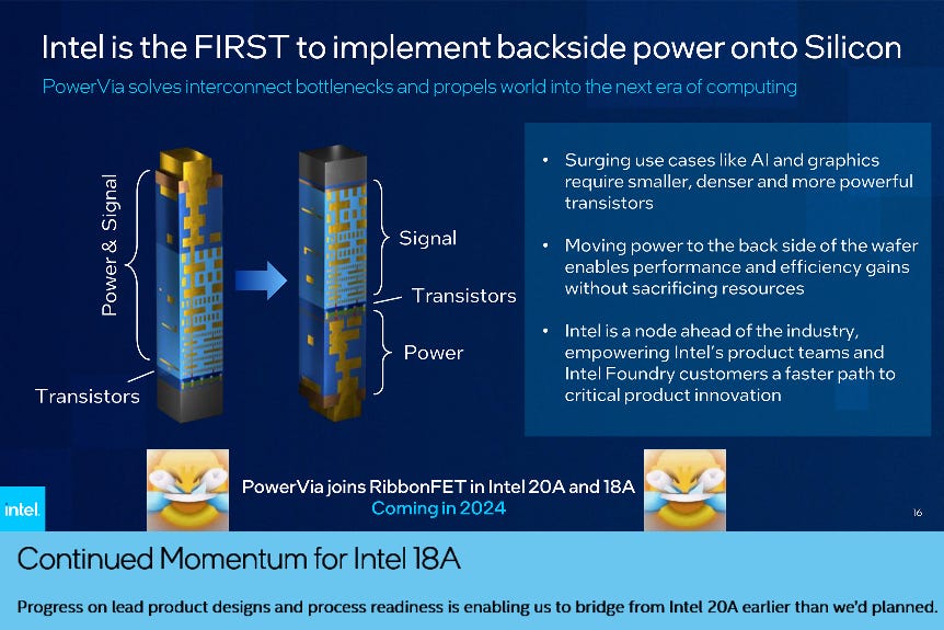
Backside-Power Delivery is a major change that has the transistors in the middle.
[5] Design Rules
Design rules are physical constraints.
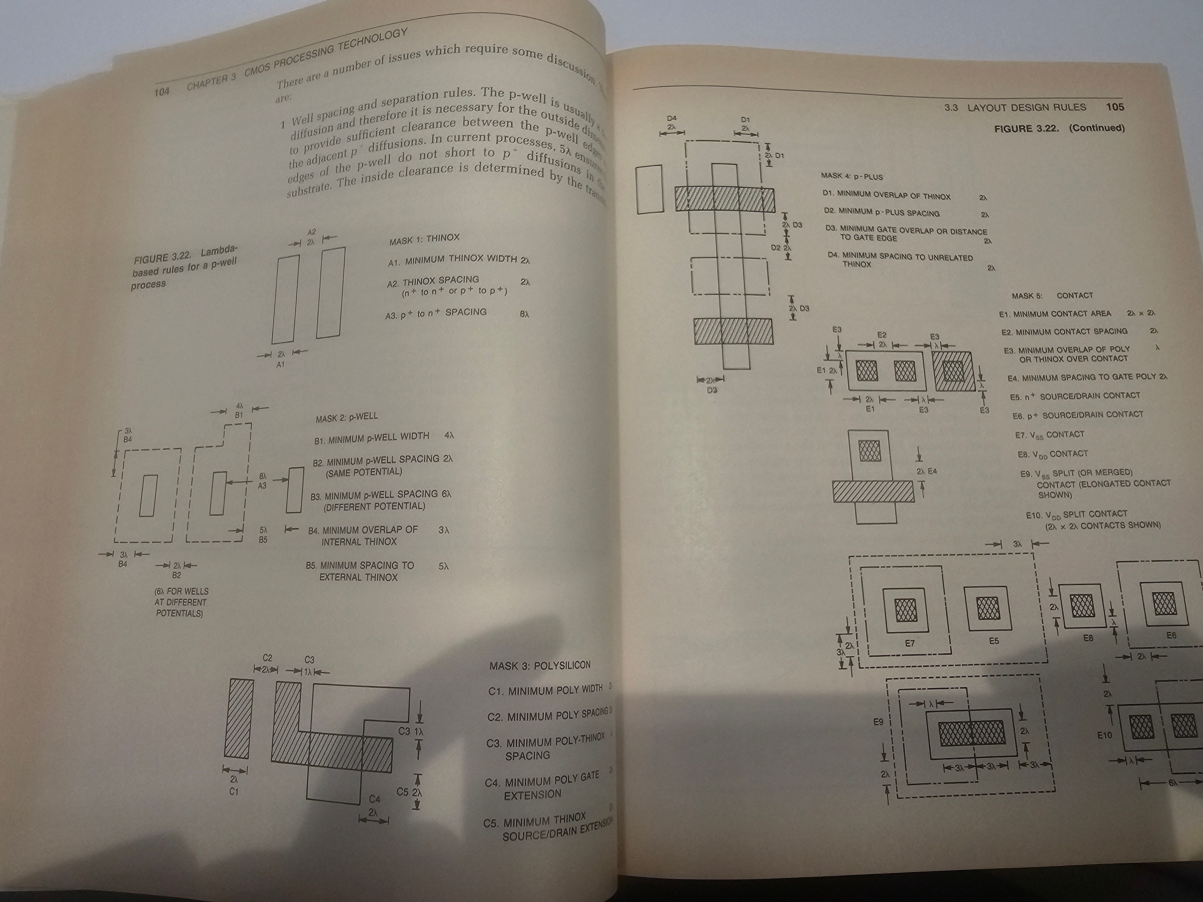
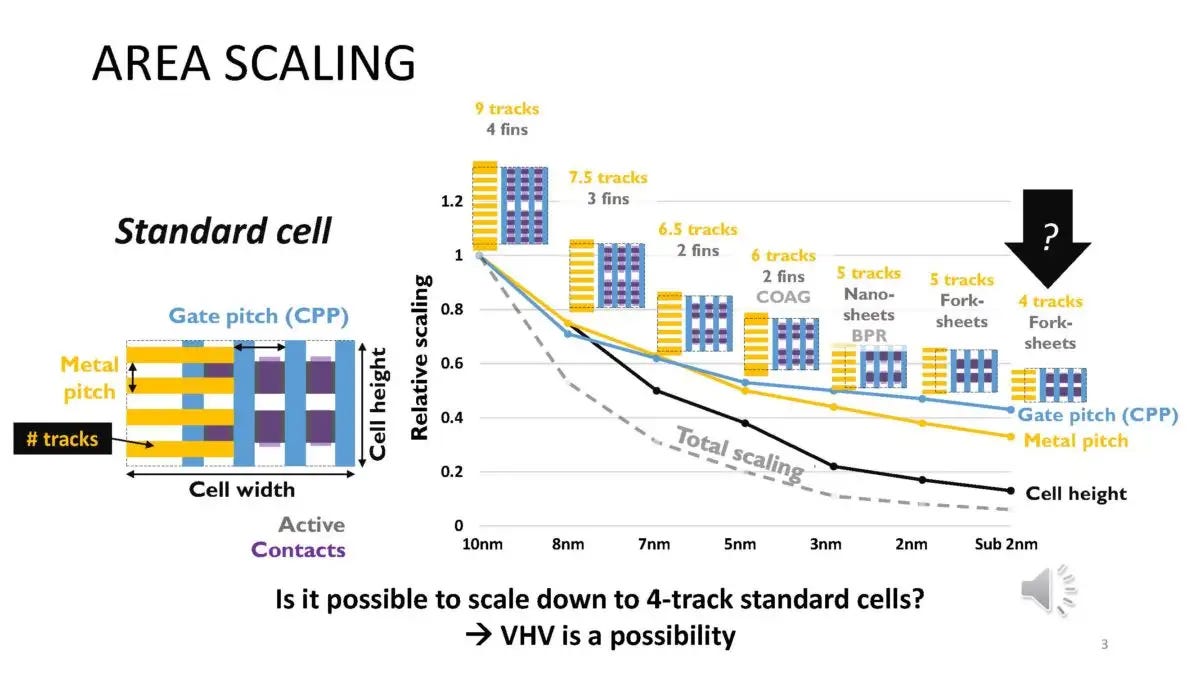
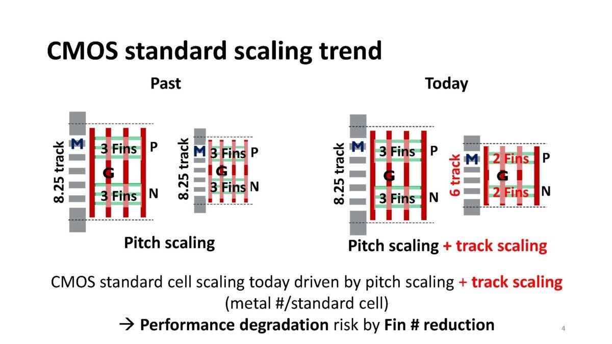
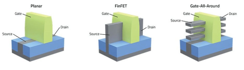
The above rules are for a basic planar process node. FinFet (~22/14nm-class through ~3nm-class) is far more complicated. Gate-All-Around (GAA) is even more complex.
Automates tools perform Design Rule Checking (DRC). It is rumored that the last time Intel tried to be a logic foundry (~2015-2018) failed because the Altera people were in charge of making design rules for external customers.

[6] Practical Issues
Section [3] went over ideal devices. Real devices have lots of unwanted attributes that cause interesting problems.
For example, clock speed and voltage of the final product are both decided after samples come back from the logic foundry.

Always remember… clock speed and voltage (by extension power/TDP) are economic choices.
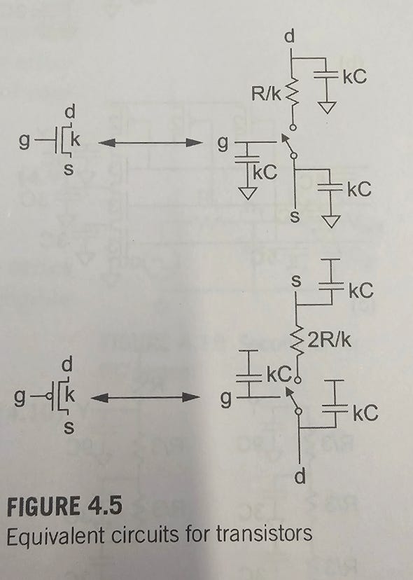
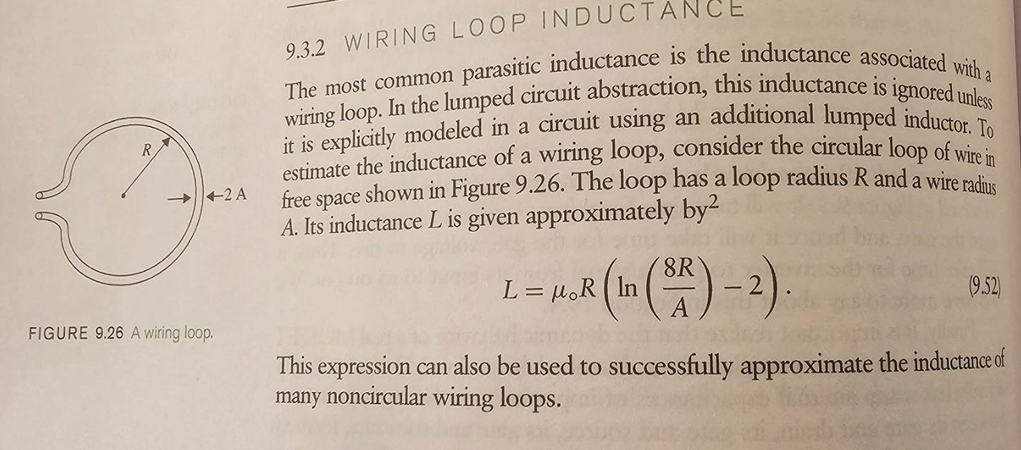
[6.a] Device Parasitics
Real devices have many parasitic (unwanted) properties. Let’s look at this basic inductor model.

Accurate and detailed modeling of parasitic behaviors for each standard cell in a PDK is critical to enabling successful design efforts.


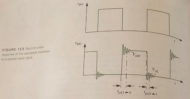
A basic inverter chain and it’s time-domain response accounting for basic parasitic properties.


A more complex model of cascaded inverter parasitics…


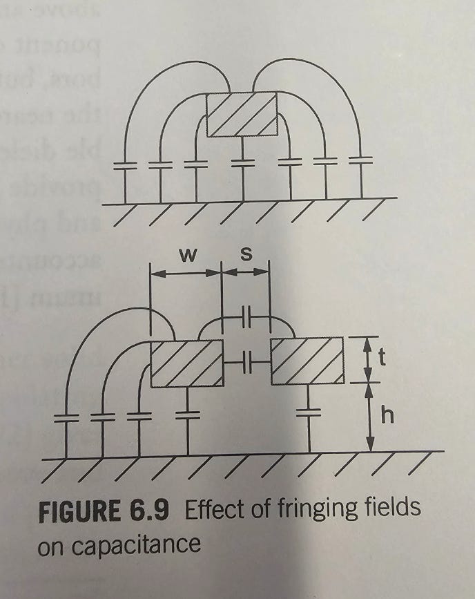
Even something as simple as a capacitor has parasitic that dramatically change it’s behavior relative to the ideal model. At high frequencies, capacitors behave like inductors (the opposite)!

Note the units. Parasitic inductance is three orders of magnitude smaller than the capacitance. Small parasitic properties lead to big problems.
[6.b] Wire Network Parasitics
Wires have parasitic properties too. It’s a big problem.


[6.c] Electromagnetic Coupling
An antenna is just a piece of metal. Wires can inadvertently become antennas.
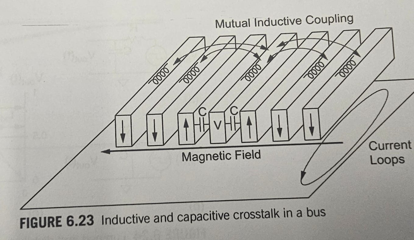
Here is a great figure on what electromagnetic coupling looks like in time-domain.

[6.d] Process Variation
Process nodes have intrinsic variation.


The industry standard method for determining parametric yield (how many chips are meet performance specifications) is by using process corners.

Designers simulate against specific process corners. Testing and tuning is done on special batches of chips (samples) that have the process corner known a-priori.
Logic Foundries run a special shuttle (batch of wafers) through the process slowly to intentionally make slow (SS), fast (FF), typical (TT), and skewed (FS/SF) parts. Specific sections of the 300mm wafer are intentionally over/under doped.
Real production wafers move thought the process steps too quickly to know which chips are what corner.
It is the logic foundries responsibility to provide accurate numbers that characterize the process corners of the node.

Some examples of how process variation effects various basic circuits.


[6.e] Temperature Sensitivity

Every device has a temperature response. Higher-level circuits such as amplifiers will have more pronounced sensitivity to temperature.
[6.f] Voltage Uniformity
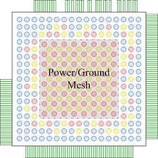
Distributing power evenly to tens of billions of transistors is… challenging.
An important standard concept is the power grid.

A chip will have many power and ground input bumps. Internally, these bumps get shorted into a grid.

There will always be variation. It must be carefully managed. If one sub-block of a SoC does not get enough voltage, you have a problem. The only easy way to fix is to boost input voltage to everything connected to the same supply rail.
(designs often have internal tuning registers to boost particular sub-circuits)
Additionally, the input DC power supply is never true DC. There is always some noise and voltage ripple.

Circuits must be designed to handle supply noise.
[6.g] Electromigration
Electromigration is how semiconductors degrade over time. Higher voltage and higher temperature accelerate the process.

Intuitively, electromigration leads to the following types of example failures:
Transistor stuck in on or off state.
Capacitor degraded. (can’t hold enough charge)
Wire thinning leading to signal integrity issues.
All those Intel 13th and 14th generation failures you may have heard about on the news are electromigration failures. Industry standard is to design and test chips such that they survive 10 years in normal operation.
Intel 13th and 14th generation (Raptor Lake) chips survive for 6-12 months. The excuses Intel has publicly stated like “oh we messed up microcode” and there is “unintended excessive voltage” are bullshit.
There exists a standardized test that is grunted to catch these kind of problems. It takes ~2 months and costs < $50K per design.
https://en.wikipedia.org/wiki/High-temperature_operating_life
Intel Products skipping HTOL testing (to save less than $100K in NRE) is their own fault. There is no excuse for such incompetence.
[6.h] Leakage and Noise
Transistors are never truly off. There will always be some leakage. (unwanted power draw)
This leakage also acts as noise for the rest of the circuit.
All devices have intrinsic noise which must be modeled by the logic foundry in the PDK.
https://en.wikipedia.org/wiki/Johnson%E2%80%93Nyquist_noise

Thermal noise is typically gaussian.

[6.i] Detailed Example: Capacitors
To bring all of the practical issues together, I found this delightful blog post from Ansys.
https://www.ansys.com/blog/difference-between-mom-mim-mos-capacitor
As an exercise to the reader, please click on the link and try to read/understand for yourself.

For the lazy, there are three main ways of building a capacitor.
There are tradeoffs.
[7] Design-Technology Co-Optimization (DTCO)

Nvidia talks about how their chips are built on a TSMC “4N” process node. This is not a typo.
Large companies like Nvidia and AMD engage in “design-technology co-optimization”. Essentially, they ask the logic foundry (TSMC) for customizations.
Examples of possible customizations:
Alternative metal stackup. (typically, more/fewer layers)
Custom cells.
Relaxed design rules.
Shifts in process to skew or move corners.

[8] Derivative Nodes
If you look at TSMC financial statements, there are some nodes missing.
Where are N6 and N4?
Logic Foundry process node names are mostly marketing nonsense these days. The “nanometer” designation is detached from reality.
The “4 nanometer” node is not 20% smaller or better than the “5 nanometer” node. Derivative nodes like TSMC N7P, N6, N5P, N4, and N4P are minor updates to the parent node.
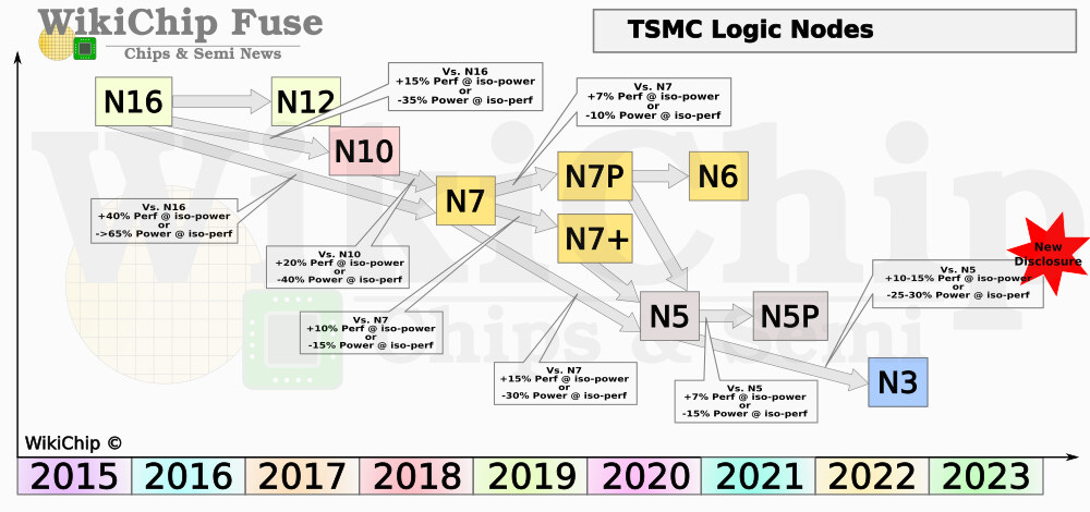
Three common tactics:
A low-single-digit lithography mask shrink.
Updated (better characteristics) standard cells in the PDK.
Relaxed design rules.
Intel’s roadmap also includes several derivative nodes.

Intel 3 is a derivative of Intel 4.
Intel 18A is a derivative of Intel 20A. This is very important and will be explained in-depth later.
As an aside, the public power/performance/area improvements publicly disclosed by logic foundries tend to be optimistic. Real designs do not get such significant improvements.
[9] Library Managment
Given the complexity of modern semiconductors, it is critical for logic foundries and design companies to manage IP (intellectual property) libraries.
Examples of IP in this context:
Standard low-level device cells.
Transistor libraries, RLC devices, via geometries, …
Can be from the foundry (PDK) or custom made (DTCO).
Low-level circuits.
PLL, SRAM, accumulator, DAC/ADC, ALU sub-units
High-level blocks.
Network on Chip (NoC) nodes
Branch Predictor
SerDes
Memory Controller
ALU/FPU core
CPU/GPU/XPU/ASIC Core
…
Typically, teams are structured in a “divide and contour” organization. It is common for individual teams to have no idea what the other groups are working on.
For very large projects, a centralized organization (let’s call them the SoC team) is responsible for taking IP block deliveries from all other groups and stitching them together into a target product.
How the centralized team interacts with other departments depends on company culture.
Some companies have back-and-forth between central team and sub-unit teams.
Sometimes the sub-unit teams deliver blocks at a hard deadline and do not really interact much with the centralized team, outside of occasional consultation.
Sometimes the overall team is so small that distinct separation within a discipline is unnecessary. For example, a unified digital team, a separate analog team (that also handles large portions of physical design), and a mask/layout team.
Regardless of the chosen structure, all teams must carefully organize IP libraries for future designs and ports to other process nodes. The semiconductor industry relies heavily on re-use of work.
In general, work can be re-used to an extent so long as nothing drastic changes.
Transistor geometry changes (planar —> FinFet —> Gate-all-Around) and innovations like backside power delivery are examples of “oh we have to re-do everything…” technologies.
Derivative nodes are very nice because they give great return on investment.
A modest amount of R&D effort translates into pretty good improvements.
It’s asymmetric.
[10] Simulations: Garbage In? Garbage Out!
A very over-simplified view of a Process Development Kit is that it’s just a bunch of numbers.
These numbers act as inputs into EDA simulations.

If the numbers are garbage, then the simulator will output garbage.


Theoretically, how can a PDK be garbage?
The numbers are lies. (intentionally wrong)
The numbers have very high variation.
Some numbers are missing, and entire categories of devices are modeled as ideal.
🤡🤡🤡🤡🤡
🙈🙈🙈🙈🙈
🙊🙊🙊🙊🙊
Certain companies think that hiding information under aggressive NDA will protect them from catastrophic failure.

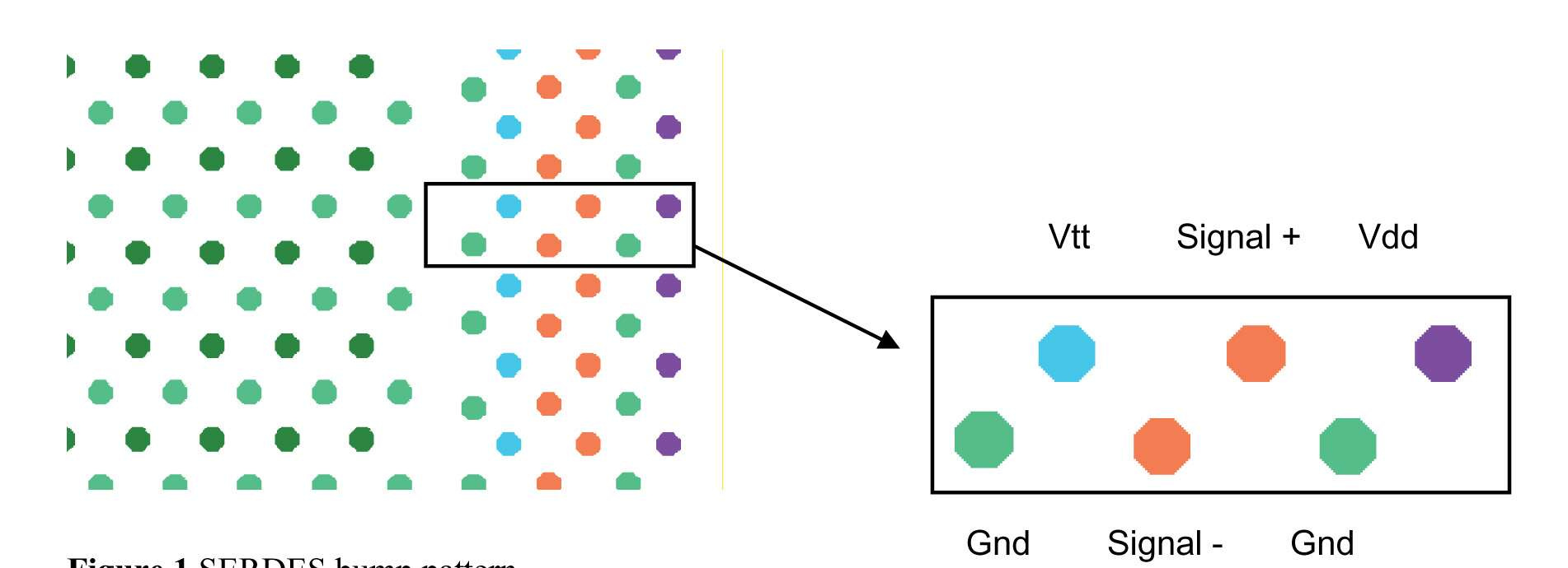
[11] Bump-Out (Packaging)
Regardless of the intended packaging, from complex CoWoS-L to basic ABF substrate, every chip needs a bump-out. Rules and specifications on where power, ground, and signal pads are.
This is more difficult that it might initially seem.
Power and ground need to be evenly distributed across the chip.
Signal wires need to be surrounded by ground to maintain signal integrity.
If too many power bumps are near each other, there will be a hot-spot.
Chip could overheat.
Warpage of the package and silicon (not same thermal coefficient) can result in the chip de-soldering itself.
Nvidia has had two run-in with bump-out related failures.
A long time ago, Nvidia made a laptop GPU that failed due to hot-spots.
To this day, Apple holds a grudge against Nvidia because of this fiasco.
Nvidia was sued and paid very low compensation to laptop OEMs.
Blackwell was delayed due to some bump-related issue.
Issue was due to aggressive timeline and adoption of CoWoS-L on Nvidia’s first chiplet design.
The upper 6 metal layers of the Blackwell logic die needed to be re-worked to re-arrange the micro-bumps.
Because bump-out is standard PDK information, companies are almost always allowed to…
Design their own package.
Choose which company (usually 3rd party) manufactures the package.
Choose which company (usually 3rd party) does the packaging. (places dice on package)
This is how the industry normally operates.

It’s almost as if insisting on non-standard workflows will lead to inefficiency, unnecessary risk, and future disasters.

[12] Overview of the three leading-edge logic foundries.
Here is an updated positions list so you know my biases.
I own a lot of TSMC shares at the time of writing.
Am I still going to own these shares ten years from now? Absolutely not.
Am I still going to own these shares two years from now? Almost certainly.

TSMC stock trades at a very low Price/Earnings multiple. This is the market pricing in the risk of an involuntary merger with SMIC.
Samsung Foundry is such a disaster, I don’t want to bother writing about them.
There is no hope.

Spend 15 minutes Google searching “Samsung yield”. Plenty of material is online from the past 7 years.
Intel is where I have to engage in some NDA-mandated memes.
I cannot write about many topics. However, public statements from Intel and public rumors are fair game. Nothing prevents me from talking about the news and chiming in with funny pictures.

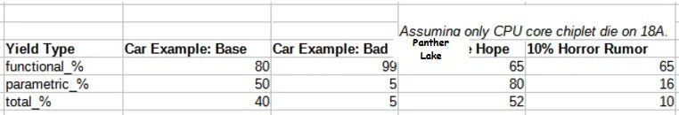
Please go check out my (1 month old) note on 18A and the rumored 10% yields of Intel Products Panther Lake CPU chiplet/tile, built on Intel 18A.
At the time, I did not have enough spare cycles to write up a detailed explanation of PDKs. This post is what I wish I could have written back then. :)


I find it immensely entertaining that the name of the Intel executive who had to put out a press release in response to Reuters reporting has the last name of “Sell”.
An Intel VP literally named “Sell” told you all you need to know. 🤣
There are two key factual claims Mr. Sell wrote on September 4th, 2024:
20A is canceled and this is actually good news!
18A, a derivative node, is yielding well with a defect density (D0) of < 0.4.

Executive officers (VP and above) of publicly traded companies cannot intentionally lie in public statements to investors.

Therefore, we have to assume that the 0.4 D0 claim is true. Presumably, Mr. Sell does not want to get sued. This is exactly the kind of claim that can EASILY be proven true/false in the discovery process.
This does not mean 18A (derivative node) is going well! Cancelation of 20A (parent node) strongly indicates that the entire node family is busted.
The following three statements can all be simultaneously true.
18A D0 is < 0.4
Parametric yield on the entire 20A/18A node family is really bad.
Rumor that Panther Lake CPU tile/chiplet on 18A has 10% overall yield.
These statements are not mutually exclusive.
Rumor is plausible in this case.
It really can be this bad.
I keep seeing technical peers in denial.
This rumor is decisively within the realm of possibility.

Regarding the rumors that some combination of Elon Musk, GloFo, Broadcom, Qualcomm, and Broadcom is trying to buy parts of intel… I have no fucking idea.
We really are on the spiciest timeline.

good comprehensive broad review of PDK. Perhaps additional chapter on content of these PDK collaterals as part of foundry enablements, such as tech files for AMS/SoC/adv package, evolution of pcells that now include many fundry process "preference" of rules, electrical and physical signoff files etc ... Each will require some kind of certification, and tsmc has been leading the industry for years, although most of design teams take foundry recommended flow as reference at the beginning of new node ramp
THANK YOU SO MUCH!!