A Guide on Semiconductor Development
How It's Made: Fancy Sand
IMPORTANT:
Irrational Analysis is heavily invested in the semiconductor industry.
Please check the ‘about’ page for a list of active positions.
Positions will change over time and are regularly updated.
Opinions are authors own and do not represent past, present, and/or future employers.
All content published on this newsletter is based on public information and independent research conducted since 2011.
This newsletter is not financial advice and readers should always do their own research before investing in any security.
Hello wonderful subscribers. Welcome to the first “deep-dive”, a category of posts that cover an engineering/technology topic with rigor while (hopefully) remaining approachable to a wide audience.
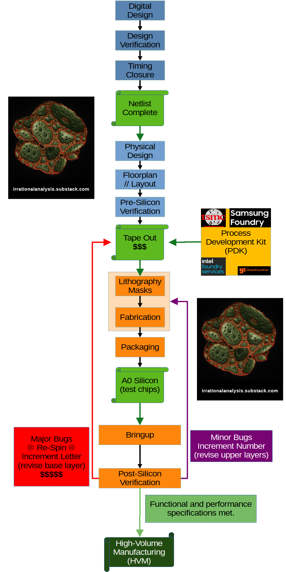
Today, we are going over the semiconductor design and product development lifecycle. Typically, it takes 2-4 years to create a leading-edge (7nm-class or lower), complex (5B+ transistor) chip from start to finish.
“Start” is defined as when the digital designers begin writing Verilog/VHDL code and “finish” is when the chip has completed post-silicon validation and is ready for high-volume, commercial production.
Ok the above flowchart might be a little overwhelming but don’t worry. We are going to make our own fake chip and follow it throughout the entire flowchart.
Digital Design:
Every chip can be defined as a series of inputs and outputs, driven by a clock signal. Chip designers target a series of specifications which can be external (PCIe 5, CXL 2.1, ARM v9, RISC-V 1.0, DDR5, HBM3, …) or internal (proprietary ISA, NVLink, Infinity Fabric, …), usually a combination of both.
In the old days, chip designers drew logic gates by hand on paper. This quickly became impractical as complexity (# of transistors) exploded.
All modern chips are designed using something called “Very Large-Scale Integration” which is a design methodology that utilizes structured rules and code. The leading hardware description languages are VHDL, Verilog, and System Verilog.
Suppose we have the following specification for our fake/trivial chip:
Objective: Periodically turn on a lightbulb if and only if two light switches are on.
Inputs:
Data Signal ‘A’
Data Signal ‘B’
Clock Input
Output: Lightbulb Power
Here is some Verilog code that describes the above specification:
module trivial_chip (

clock,
A,
B,
lightbulb

);

input clock;
input A;
input B;
output lightbulb;

always @ (posedge clock)
begin

lightbulb <= (A && B);

end

endmodule
HDL code needs to be converted into logic gates and (eventually) transistors. This process is called synthesis and is somewhat analogous to compiling C/C++ code into assembly using GCC/LLVM.
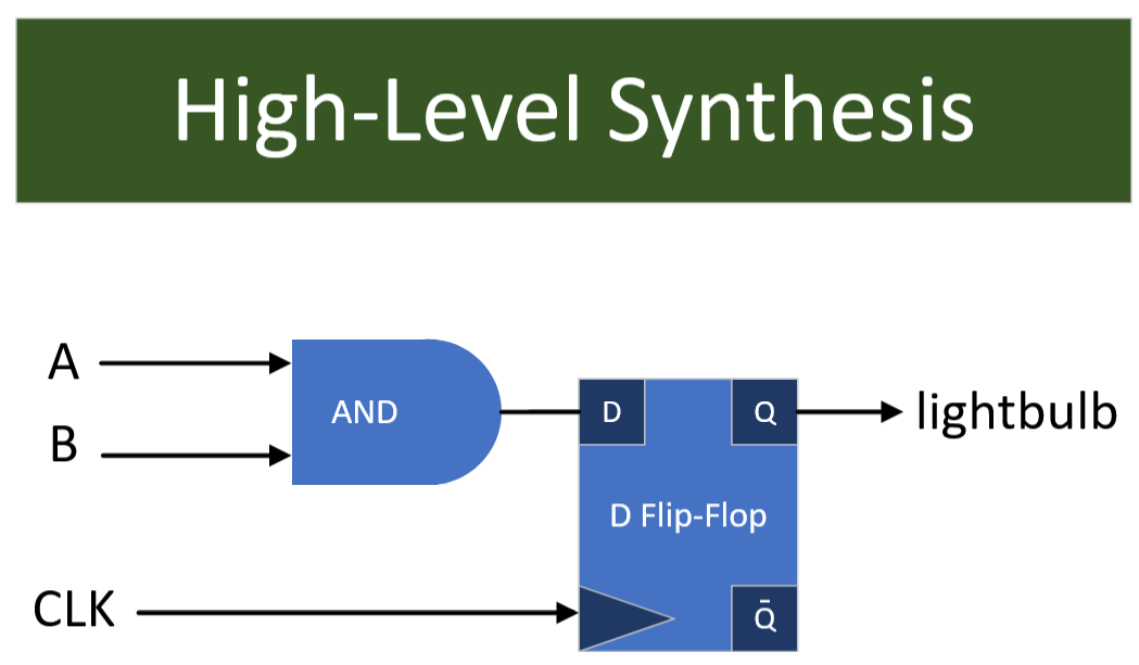
Synthesis of the above Verilog code would look something like this:
First, the design is synthesized into high-level blocks. Flip-flops are memory cells that are updated on the rising edge of the clock signal. There are many other high-level blocks that designers use for abstraction. It is very common for IP (intellectual property) to be abstracted as a macro/block.
Some examples:
CPU Core Microarchitectures (ARM X3, AMD Zen4, Intel Golden Cove)
Interconnect PHYs
Memory PHYs
VLSI design is all about “divide and conquer”. Each team controls their own respective blocks and delivers to a central SoC (system on a chip) team that builds the final chip/product. IP re-use is important to keep costs down.
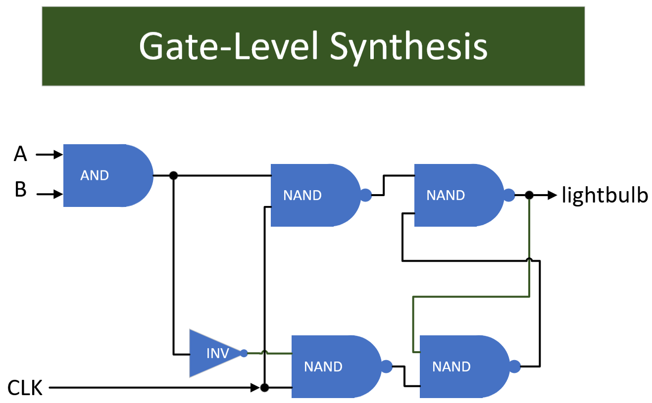
The D Flip-Flop can be further broken down into logic gates. Once the entire design has been broken down to gate-level, the synthesis tool can perform some optimizations and reduce gate count. It is common to convert as many logic gates as possible to NAND/XOR to improve manufacturability.
Design Verification:
We now have a gate-level model of the design and need to check it for flaws. This process is called verification and has become quite challenging.
For more information on verification, I highly recommend Jon’s post/video.
In a nutshell, complex designs need to be mathematically “proven” correct. Edge cases, bugs, and design oversights can become major, expensive problems if they are not caught at this stage of development.
One example is the legendary Intel Pentium FDIV bug.
Certain Intel CPUs were discovered to calculate floating point divisions slightly incorrectly approximately 1 out of 9 billion calculations.
Sounds like a minor problem, right? Intel’s marketing department tried to spin it that way.
On January 17, 1995, Intel announced a pre-tax charge of $475 million USD, equivalent to $953 million USD in 2023 dollars. They had to recall and replace all the effected CPUs.
Seemingly small problems missed in design verification can lead to big financial consequences later on.
Timing Closure:
Now that the design has passed verification and is believed to be “mathematically correct, the challenging process known as “timing closure” begins. Each digital logic element (logic gates, mux, flip-flops, …) has its own delay, measured in clock cycles. For example, it might take one clock cycle for a flip-flop to update but three clock cycles for a NOR gate to update. Within each design, these delays must be accounted for in relation to various reference clocks.
Chips typically advertise their primary (base) clock in marketing but there are hundreds to thousands of internal clocks that run throughout the chip. Clock dividers, phase-locked loops, clock multipliers and such use the base clock to generate other clock signals.
An easy way to complete timing closure is to find the longest delay within the circuit (critical path) and simply add time delays on all other paths via inverter chains. Of course, this is inefficient, so design teams spend a great deal of time adjusting aspects of the logic circuit to simultaneously minimize and align all the clock signals. For example, a floating-point math unit (FPU) might be too slow and is unable to keep up with the scheduler under simulated workloads, so the designers widen the FPU and re-structure the internals to improve latency and eliminate the bottleneck.
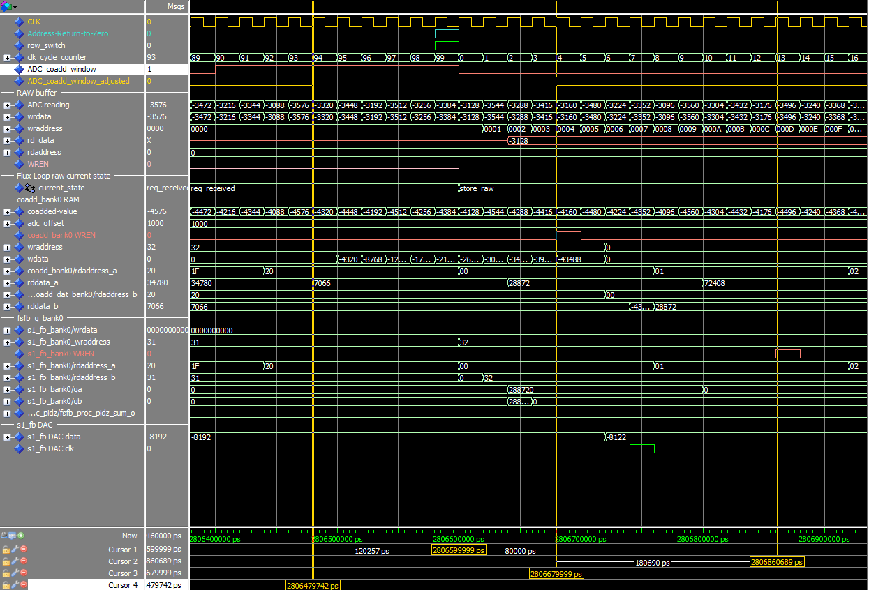
Timing closure is an important milestone which leads to the first deliverable within the semiconductor design cycle.
Milestone #1: Netlist
At this point, the digital design team have done their jobs and typically move on to the next project. Before beginning work on the next generation design, they deliver the in-progress generations netlist to the physical design team. A netlist is a “compiled” representation of the design represented by a large network of inputs and outputs. It is somewhat analogous to compiled binary blobs of assembly code.
Companies sometimes refer to netlists internally or externally as “IP blocks” (intellectual property, IPs) because they are regularly re-used and sometimes licensed out.
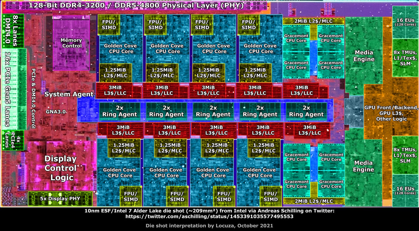
Above is a labeled block diagram of an Intel client (laptop) chip. The big CPU core design (Golden Cove) is re-used for Intel’s server chip codenamed Saphire Rapids. A few modifications are made (slightly different cache configuration) but the design block is largely re-used from the original netlist delivered by the Golden Cove team.
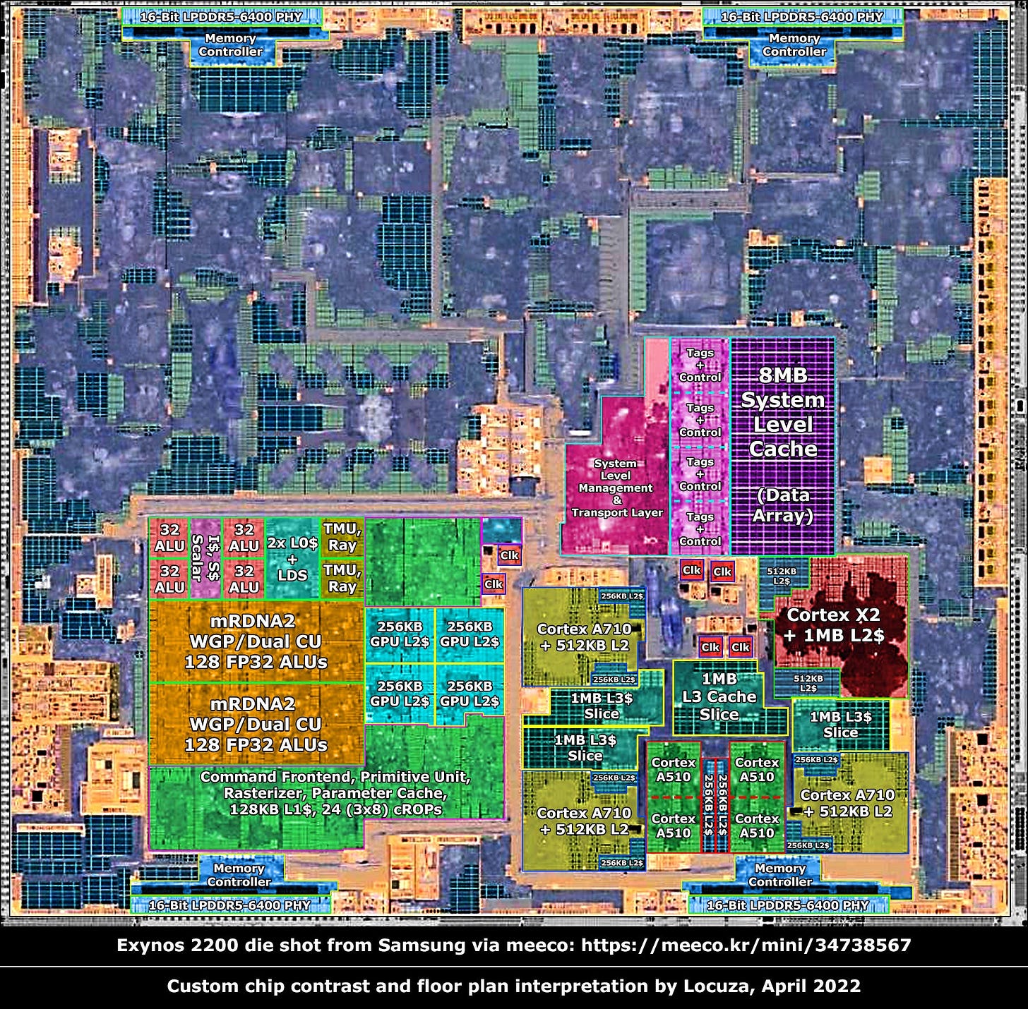
Another example is the Exynos 2200 created by Samsung LSI (S.LSI). Here, the GPU IP (RDNA2) is licensed from AMD in the form of a netlist. CPU IPs are also licensed as netlists from ARM (LTD) under the Cortex public branding.
Physical Design:
Real chips are physical objects made of transistors, resistors, capacitors, inductors, diodes, and so on. The netlist needs to be converted into real-world circuit by the physical design team.
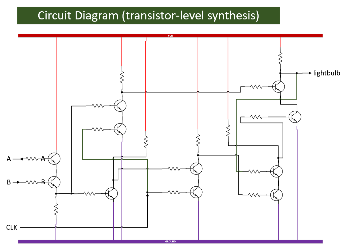
Oure fake/trivial chip will look something like this:
Notes:
Real, high-performance chips need filtering elements (typically very small capacitors) to smooth out internal frequency responses.
I will be removing all the resistors in future diagrams to reduce visual complexity.
We now have a physical circuit with power (voltage rail // VDD), ground, inputs (A, B, CLK), and output (lightbulb).
Floorplan // Layout:
The above circuit diagram would be easy to build on a breadboard but complex chips with tens-of-billions of transistors need to be printed using a process technology. This is a fascinating topic of its own and outside the scope of this post.
<>
For now, here are the basics:
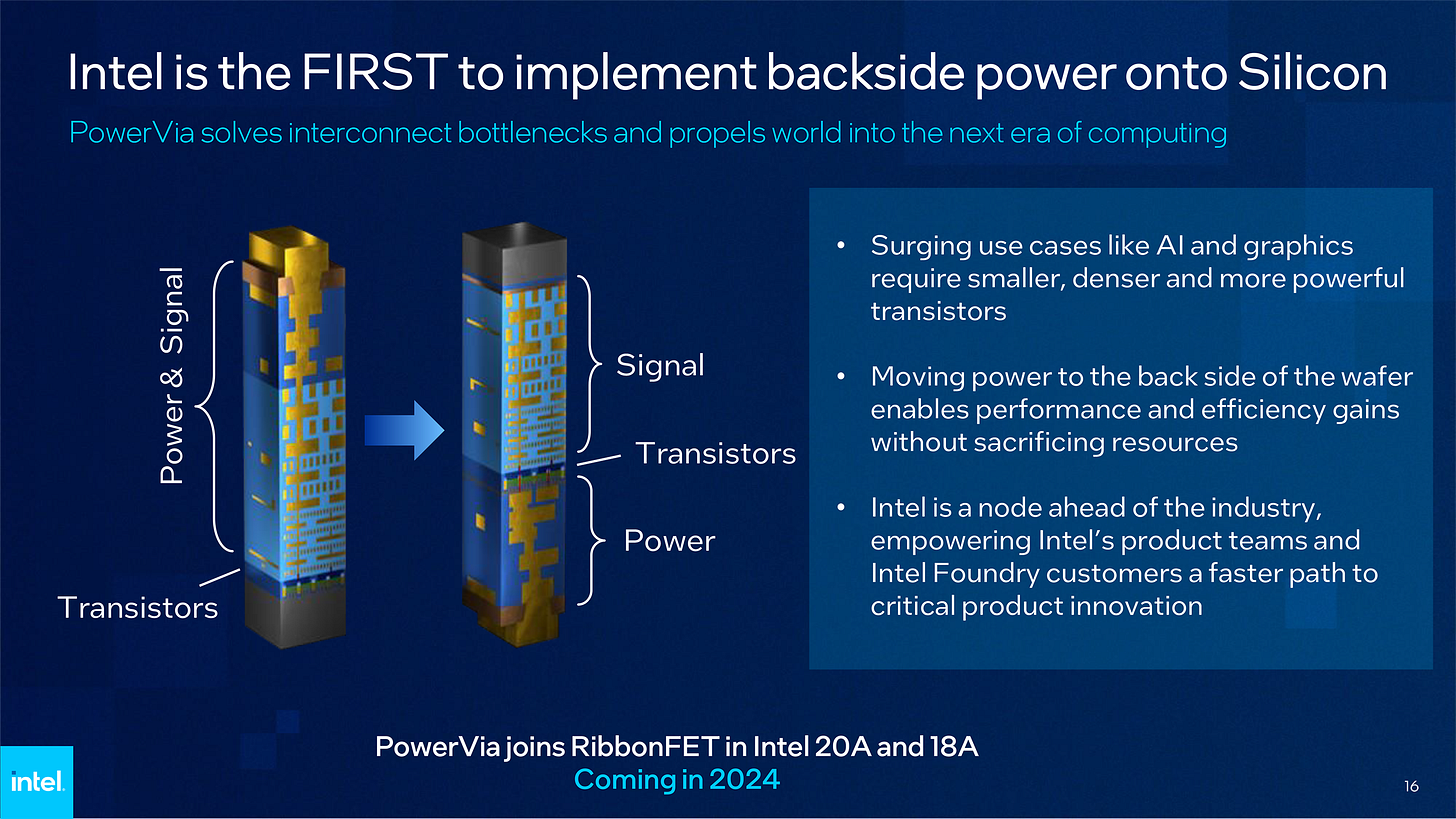
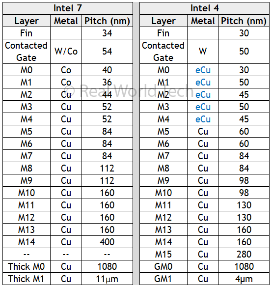
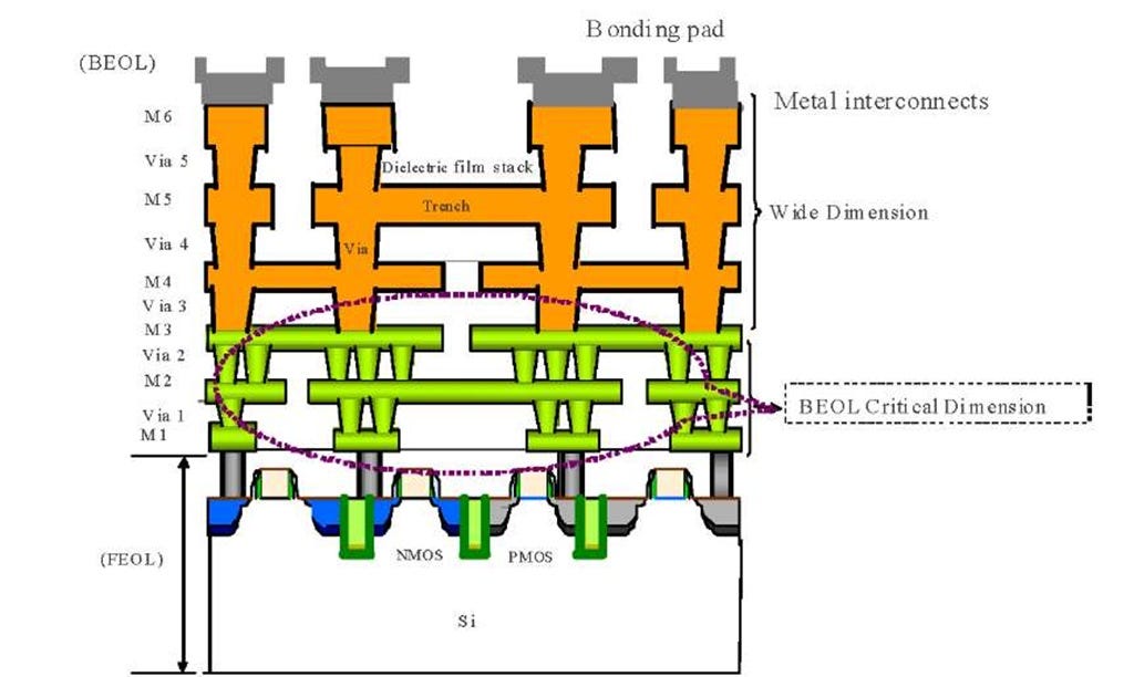
Chips are made of layers where the bottom layer (M0) contains all the transistors, and each layer above contains wires of increasing width. This will be changing next year with Intel’s backside power delivery. For more information, I highly recommend reading Doug’s writeup on the topic.
Each layer is connected to the next using “VIAs”.
These are essentially vertical wires and are needed because wires in the horizontal plane cannot overlap one another within the same layer. This leads to a challenging series of constraints/problems.
We don’t want wires to be too long as that will burn a lot of power from resistive losses and reduce circuit speed due to increased delay.
We can’t put certain wires too close together as electrical noise will corrupt neighboring signals.
Wires carrying power need to be spread out to avoid creating hot spots on the chip.
Input/Output ports (PCIe, USB, memory PHYs) need to be on the edge of the chip but can’t be too far away from processing cores.
Transistors are provided by the PDK in various library groups at different speed/power/performance characteristics.
…
The physical design team has to balance all these factors using the “PDK” (process development kit) provided by the foundry and deal with this routing hell.
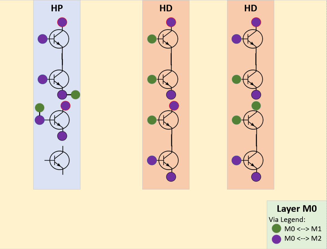
Let’s convert our fake/trivial chip into a real physical design using a fake process node that has the following attributes:
There are three layers, one base (M0) and two wire (M1, M2) layers.
The fake PDK provides two transistor libraries.
4x fast, high-power transistors (HP)
4x dense, low-power transistors (HD)
Flip-chip packaging requires all I/O to ingress from the top layer. (more on packaging later)
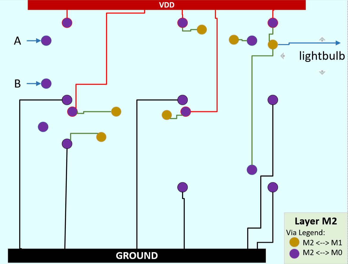
Our fake chip will be implemented on the fake process node as follows:
Highlights:
No wires cross over each other on the same layer. (important!)
All the transistors are on the bottom layer.
There is an extra transistor because our fake PDK only has libraries with 4x transistors per cell.
This is a good thing.
Extra transistors enable future “patches”.
(more on this later)
All the external signals (input, output, power, ground) are on the top layer. (more on this later)
Pre-Silicon Verification:
We now have a physical design but need to go through one last verification step. But wasn’t verification already done earlier?
Design verification (DV) and pre-silicon (Pre-Si) verification are distinct steps.
DV checks for the mathematical correctness of the design.
Pre-Si verification checks for the “physical” correctness.
What does this mean…?
Some examples:
Two signal wires might be too close together and certain workloads may cause leakage/noise to flip bits, breaking the circuit.
A group of transistors might generate hot spots under heavy workloads, leading to degraded performance or even chip failure due to cracking.
Simulations based on the latest PDK version might suggest poor yields and necessitate the use of different/updated transistor libraries (cells) to mitigate.
…
Pre-silicon verification is extremely important because it is the last chance to spot and fix problems in simulations before the next, very expensive step…
Milestone #2: Tape-Out
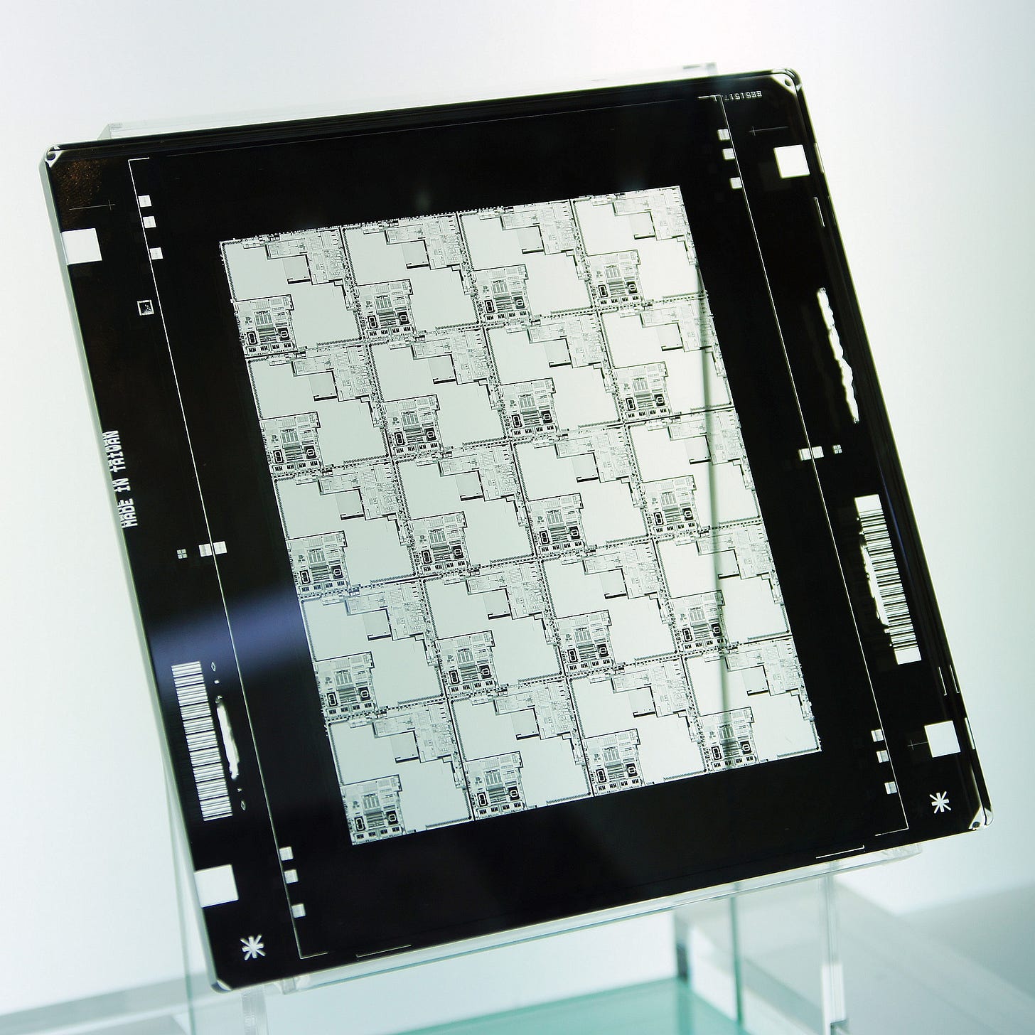
The finalized physical design is ready and is now sent to fabrication partners. This process is called “tape-out” and costs 20-50 million USD for leading-edge (7nm-class and lower) process nodes. The Fab begins preparation and lithography mask suppliers (typically companies other than the Fab itself) create expensive mask sets.
Each layer of the chip needs a lithography mask, sometimes two or four masks per layer (multi-patterning). Light is shined through the mask to mass-print the design upon the wafer. Remember that the transistors are on the bottom/first layer and wires are on subsequent layers. This will be important.
Modern process nodes have ~15 metal layers and 80+ total layers. Thus, it takes a long time for each wafer to go from start to finish. Leading-edge (7nm-class or lower) process nodes have a lead-time of 3-6 months, depending on a variety of factors.
This is why pre-silicon verification and tape-out are so important. If there are any mistakes, you only find out **months** later.
Packaging:
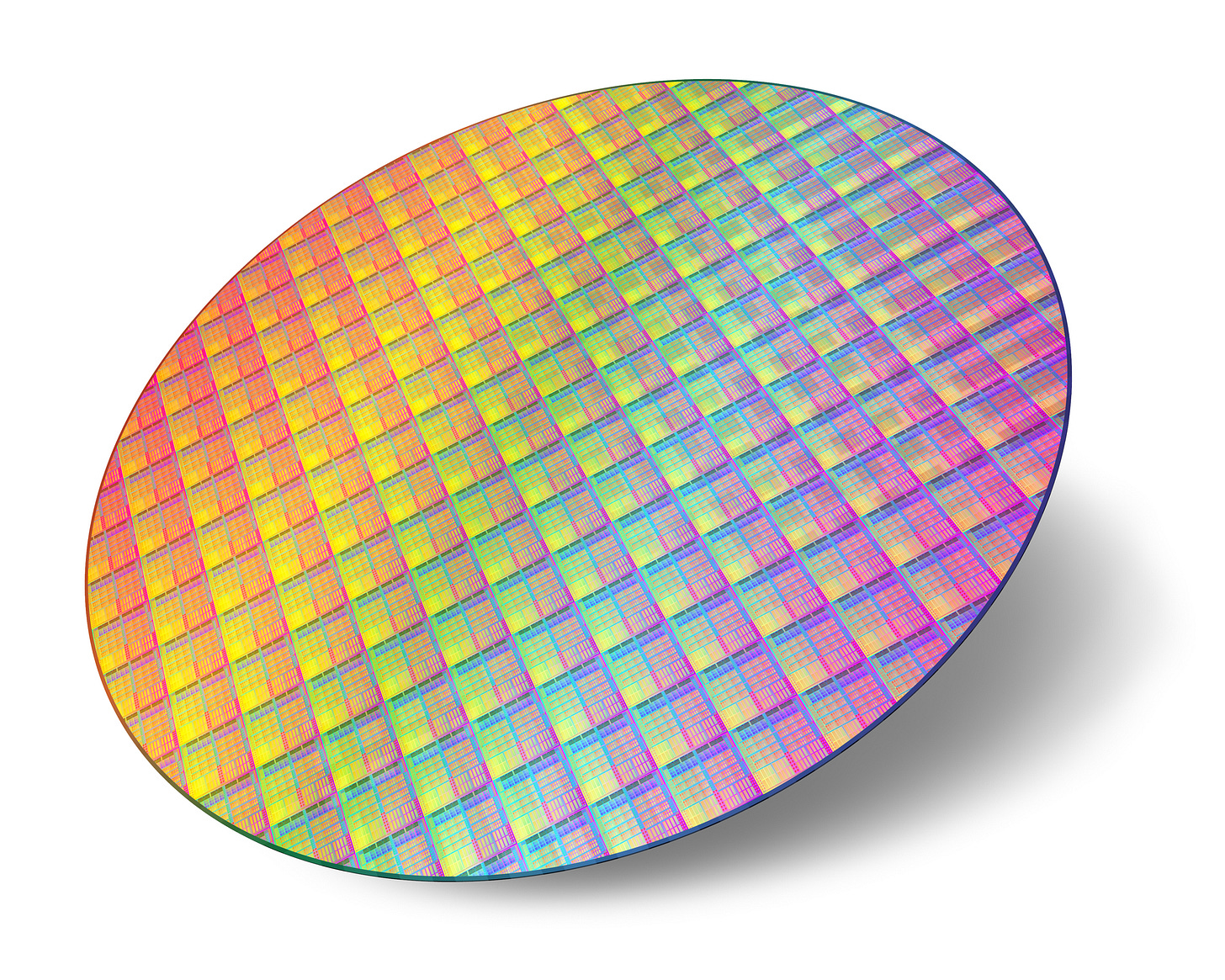
Once the wafer is done, it will look something like this:
Many copies of the same design need to be chopped up and packaged to become usable for testing and (eventual) commercial sales.
There are many types of packaging, and this design step is rapidly becoming more important due to chiplets, HBM, SRAM/analog scaling issues, and so on.
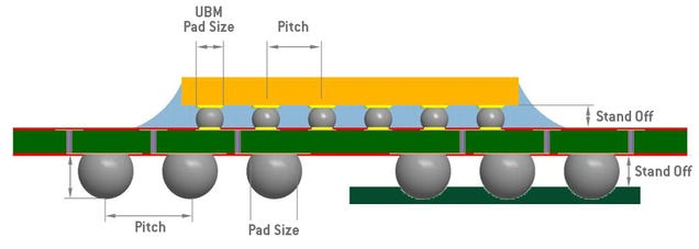
The cheapest and most common form of packaging is called “flip-chip”. Semiconductors are printed “bottom-up”, with transistors first. To package, the diced chip is flipped onto a plastic or organic substrate to increase surface area for I/O pins.
Tiny solder balls can then be used to place the package onto a larger board/PCB.
For more information on packaging, I highly recommend reading Dylan’s series on the topic:
Milestone #3: A0 Silicon
After months of waiting, the initial (small) batch of test chips come back into a lab. This is an exciting time where many teams of engineers band together in pursuit of one task: turn the chip on and check basic functionality.
Bringup is the industry term for this step and involves going through a long checklist of functional requirements. Often, there are bugs that break certain functional blocks or prevent stable operation. Sometimes, the chip won’t stay on and keeps locking-up, crashing, or becomes unresponsive.
Once the bringup team has figured out how to stabilize the chip, the next phase of the design process commences.
Post-Silicon Verification:
When you have billions of transistors on a chip, it is inevitable that things will go wrong. It is for this reason that all chips are full of internal tools/knobs that allow engineering teams to debug, tune, characterize, and analyze the functionality and performance of each sub-system.
Some examples:
“Chicken bits” that can be programmed or enabled via dipswitches.
These bits typically disable new features, reducing complexity and enabling easier debugging.
JTAG
A mechanism where debug information can be read directly off of the chip and allow for low-level configuration of internal chip systems without an operating system or even firmware.
Analog Sources
Internal current sources and/or voltage multipliers can boost problematic signals (at the cost of power consumption) to allow for further debugging.
Configuration and Debug Registers
These are internal registers that do not have public documentation, allowing engineers to read detailed information and enable/disable a wide variety of functionalities. For example, disable a security feature by writing to a debug register and read proprietary information about low-level functionality within the design.
After analyzing the performance and functionality of the A0 silicon, a decision needs to be made.
If the chip passes, the design company gives a green light to the Fab and requests mass production. It is exceedingly rare for A0 silicon to enter high-volume production due to the incredible complexity of modern semiconductors.
If there are minor problems, the design teams can revise wiring on higher layers to “patch” the bugs. Designers like to keep extra transistors and circuits available for redundancy and optionality to patch bugs. If this happens, the number of the chip revision is incremented (A1, A2, A3…) and it induces modest costs upon the design company. Suppose a “patch” can be applied to the top metal layer. The Fab can take an in-progress, almost-finished wafer and use a new lithography mask for that last layer. The design company needs to pay for an extra lithography mask (not a whole set) and only needs to wait ~one month instead of the full 3-6 months.
If there are major problems, the chip must undergo a “re-spin”. This industry term means a bug/issue is so severe, it must be fixed in the base-layer, incurring huge costs upon the design company.
ALL the in-progress wafers are junk and must be thrown away.
Post-Si validation team must wait 3-6 months before new test chips are ready.
Tape-out has to be done again, incurring tens-of-millions of dollars of cost. (again)
The products time-to-market is delayed by at least 3 quarters, leading to opportunity cost for the business.
Silicon ages like milk.
A design that was competitive in year X can become utterly uncompetitive in year X+2.
Intel Sapphire Rapids was delayed by 2-years due to repeated re-spins, resulting in E5 silicon finally shipping in commercial volume.
Again, it is very rare for A0 silicon to ship. Usually B0/B1/B2 is what gets shipped. One re-spin is somewhat expected these days. Four re-spins (Intel Sapphire Rapids) is exceptionally poor and indicates severe organizational issues.
Sidenote: Intel held a webinar about their (in-progress) internal foundry model and I hope to write a detailed post about Pat Gelsinger’s progress at some point.
<>
And with that, we are at the end of the first deep-dive. Hopefully, the above flow-chart makes sense.


