Brief Intel 18A Yield Note
What the rumors really mean.
Irrational Analysis is heavily invested in the semiconductor industry.
Please check the ‘about’ page for a list of active positions.
Positions will change over time and are regularly updated.
Opinions are authors own and do not represent past, present, and/or future employers.
All content published on this newsletter is based on public information and independent research conducted since 2011.
This newsletter is not financial advice, and readers should always do their own research before investing in any security.
Feel free to contact me via email at: irrational_analysis@proton.me
Contents:
Intro
A Car Analogy
Intel Panther Lake Rumor
Possible Outcomes
Moronic Rorschach Test
[1] Intro
There is this 10% yield rumor for Intel 18A making the rounds.
First, the 10% yield rumor is coming from Korean press, full of delusional Samsung Foundry sympathizers.
Second, the Broadcom test chips were on PDK v0.7 so nitpicking this is a waste of everyone’s time.
Finally, almost everyone discussing this topic either has no idea what they are talking about or choses to selectively explain the situation.
[2] A Car Analogy:
I will explain semiconductor yield with a car analogy.
Suppose you have a car factory. The cars are marketed with the following three parameters:
Maximum cruising speed (mile-per-hour, MPH)
Fuel efficiency at cruising speed (miles-per-gallon, MPG-F)
Fuel efficiency in city driving (miles-per-gallon, MPG-C)
Many stops and starts at lights and stop signs.
Low (5-30 MPH typical speeds)
The semiconductor version of this analogy is:
Clock frequency at load. (F_MAX, all CPU/GPU cores working)
Power draw at load. (P_MAX, watts)
Power draw at idle/light load. (P_IDLE, some cores working)
A weighted average of real scenarios based on the target market and product type.
Some cores active, lower power state, some IP blocks off, …
For a car to be considered functional:
The engine must turn on.
The brakes must work with a minimum stopping power. (too low is a safety risk)
The engine must not fail due to overheating.
Let’s say 80% of all cars produced the factory are functional.
In order to be competitive in the market, the product management and market research teams looked at competitors roadmaps and rumors and determined a set of goals.
60 MPH max cruising speed.
80 MPG efficiency at max cruising speed.
70 MPG efficiency for city driving.
Suppose 50% of cars produced by the factory meet these specifications. They can be sold as planned, without issue.
Thus, the overall product yield of the car factory is 80%*50% = 40%.
Suppose you build a second factory that outputs 99% functional cars, but the parametric yield is terrible. Only 5% of cars meet spec.
The other 95% have like 20 MPH max speed before overheating. They also guzzle gas, achieving a pitiful 30 MPG at high speed and 10 MPG in city driving.
You cannot sell this garbage. Nobody will buy it. Competition is much better.
[3] Intel Panther Lake Rumor
Real rumor is this:
Panther Lake CPU core chiplet allegedly has overall yield of 10%.
Intel cope on Twitter has people using the 0.4 defect density (D0) advertised by Intel publicly as a way of claiming this rumor is impossible.
Let’s do some quick math to illustrate why this rumor is absolutely plausible.

As you can see, parametric yield matters a lot.
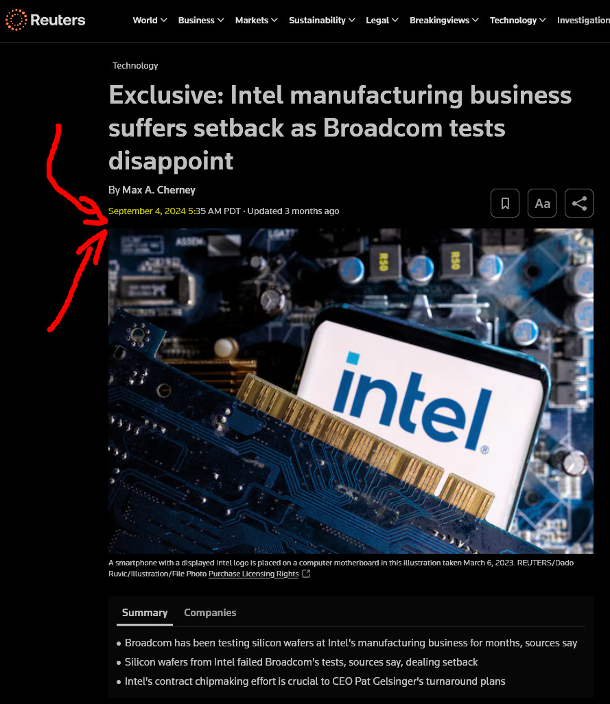
I would like to remind everyone that this 0.4 defect-density number came in response to a Reuters report. Published on the same day.
D0 is a closely guarded secret.
TSMC has previously published D0 trend but stopped.
There are no public or official D0 numbers for TSMC N3B (failed node) or TSMC N3E/P (very good node family).
Ask yourself why Intel felt the need to publish 18A D0 on the exact day they knew negative press was coming.
It’s because the average investor does not understand what parametric yield is.
[4] Possible Outcomes
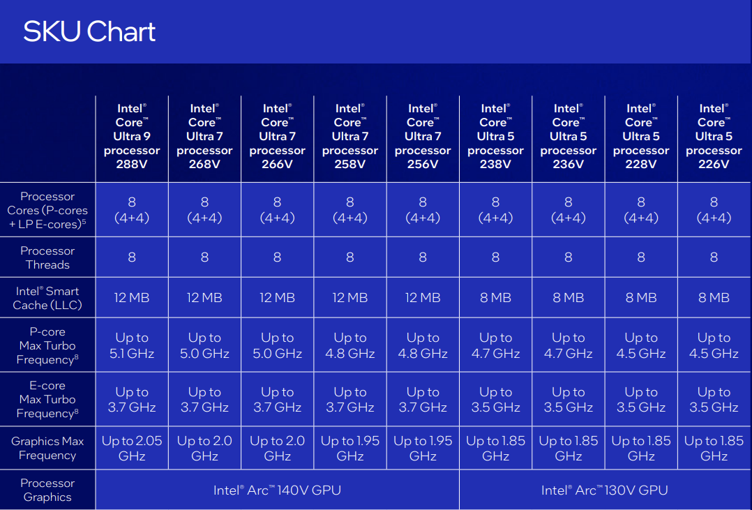
Let’s take a look at the Intel Lunar Lake SKU stack.
Within semiconductors, there are two ways to “yield harvest”.
Disable parts of the chip (typically CPU/GPU cores).
Limit parts of the chip (typically CPU/GPU cores) to a lower clock frequency.
Intel, AMD, Nvidia, and many other semiconductor companies use yield harvesting. Certain consumer products, laptop/PC chips in particular use this tactic aggressively to maximize number of sellable chips.
In this most recent example, Intel product management and competitive analysis groups looked at silicon data reports and made several decisions.
A lower tier set of products will have a small number of functional blocks disabled.
Slightly fewer GPU cores.
33% less SRAM.
Each descending SKU will have slightly lower CPU and GPU core speeds.
Every design team runs simulations to estimate expected functional and parametric yield. The product management team uses this information alongside competitive market intelligence (guesses on what the competition will release) to set goals for designers.
These simulations depend on the process-development kit (PDK).
If the PDK is wrong, the simulations are way off and reality hits hard.
Here are the options:
Panther Lake re-spin and delay launch by 4-6 months minimum. Hope PDK is accurate this time.
Keep the existing power and performance goals, destroying gross margins.
Lower goals, release a slow product with underwhelming battery life, get beaten to a pulp by the competition (AMD, MediaTek/Nvidia, Qualcomm).
There are non-engineering ways out of this mess. (#2 and #3)
[5] Moronic Rorschach Test
Have you ever seen one of these?
This is called a Rorschach test.
Psychiatric patients are asked “what do you see” when shown various inkblots.
For what it’s worth, I see a butterfly made of pine trees.
The current Intel 18A 10% yield rumor cycle feels like a Rorschach test.
Koreans/Samsung people see that Intel Foundry is failing just as hard as they are.
Intel fans cling to the 0.4 D0 number as if it will ward off the epic annihilation that is coming from this rumored disaster, if true.
Pat Gelsinger (praise be upon him) is posting on Twitter (he has some free time these days) trying to correct poorly informed non-technical people without describing the full situation.
Gelsinger is smart enough to know the difference between parametric and functional yield.
Like many in this industry, he is aware that Samsung Foundry has terrible parametric yield.
TSMC engineer meme accounts are also trolling without telling the full truth. That 60% alleged yield on TSMC N2 is probably a single ARM A72 (tiny) core with very relaxed PVT constraints.
We will find out next year what the parametric yields of Intel 18A are.
It shall be such fun.


As lithos on twitter pointed out, it seems the original source isn’t the Korean press but actually New York Times which the Korean site just parroted -
https://www.nytimes.com/2024/12/02/technology/intel-ceo-pat-gelsinger.html
“TSMC is producing 30 percent of its leading-edge chips, known as 2 nanometer chips, without any flaws, while Intel’s new process produces less than 10 percent of its 18a chips without flaws, the person said.”
I agree with the other comment that the anonymous source is likely referring to Broadcom as it talks about “customers” which I doubt Intel product will be referred to as.
I think we can afford NYT some more journalistic credence. While we have no idea what the parameters of the 10% on 18A vs 30% on N2 is, one would hope that they know enough to verify that like things are being compared.
Given that, what do we make of it? One take is that BSPDN is more complicated so one would expect Intel to be a bit behind. But how much? The other possibility is that this is the reason why the board decided to fire Pat since it’s not doing as well as N2 so far and they have lost patience and don’t want more bad news to come out without them seemingly doing anything about it.
Nice car analogy