


NVLink Fusion: Jensen Murders UALink with Galaxy-Brain Strategy
Custom AI silicon landscape re-shaped. Massive winners and losers.

Irrational Analysis is heavily invested in the semiconductor industry.
Please check the ‘about’ page for a list of active positions.
Positions will change over time and are regularly updated.
Opinions are authors own and do not represent past, present, and/or future employers.
All content published on this newsletter is based on public information and independent research conducted since 2011.
This newsletter is not financial advice, and readers should always do their own research before investing in any security.
Feel free to contact me via email at: irrational_analysis@proton.me
Mr. Leather Jacket has once again outsmarted his ennemies.
The recent announcment of “NVLink Fusion” is an incredible strategic move that has re-shaped the entire AI ASIC market.
To understand why, we need to go into technical details.

Contents:
PHY vs Protocol
Explanation of the Announcement
IEEE 802.3ck/dj KR vs VSR vs Nvlink C2C vs NVLink5
Reach and Tradeoffs
Why “Open” is not Necessarily Better
Practical (Visual) Overview
Strategic Impact
Nvidia
Synopsys, Cadence, and Alphawave
Broadcom
Alchip, Marvell, and Amazon
Astera Labs
MediaTek and Google
Fujitsu and Qualcomm
AMD and Other UALink **LOSERS**
[1] SerDes vs Protocol
Communication links are divided into layers. There exists a standard model called OSI.

You don’t need to understand this entire mess. PHY means “physical layer”, which is often referred to as SerDes. This is the analog hardware that moves raw bits from point A to point B. Everything above the PHY is digital logic or software for managing higher level functions.
Every interface you are familiar with (Ethernet, PCIe, HDMI, USB, HBM, DDR) has a PHY and “the other stuff”.
The PHY is the differentiator.
Only two companies have high-quality 200Gbps SerDes PHYs.
Nvidia and Broadcom.
NVLink5, NVLink C2C, AMD Infinity Fabric, Ethernet, InfiniBand, UALink, Broadcom Scale-Up Ethernet, PCIe, and so on are terms that refer to the PHY, upper layer, and entire stack… interchangeably. This leads to unfortunate confusion.
For example, NVlink5, Ethernet and InfiniBand are structurally very similar at a PHY level.
AMD Infinity Fabric is structurally similar to PCIe.
UALinik and Broadcom Scale-Up Ethernet official specs literally say the PHY shall be IEEE 802.3dj Ethernet.


Remember that PHY quality is the real differentiator. All the other stuff is low-value digital and software plumbing that any semi-competent team can implement.
In other words, UALink can only be as good as the Ethernet PHY implemented by the customer.
Given that neither Nvidia or Broadcom are actively participating in UALink, there exists no high-quality option on the market.
[2] Explination of the Announcment
Ryan Smith (on behalf of ServeTheHome) made an excellent diagram explaining what is actually happening.

NVLink C2C (short range 200G SerDes) is now open to license as an IP block to third parties. This means partner companies can add this hardware directly to their chip design.
NVLink5 (long range 200G SerDes) IS NOT LISCENSED. Nvidia will be selling a “fusion chiplet” that has NVLInk C2C on one end and NVLink 5 on the other. Intuitively this is an asymmetric re-timer. One SerDes go in, other SerDes go out.
Long-reach SerDes IP critical to Nvidia’s moat IS NOT LISCENSED. This block is only available on the fusion chiplet made by (and fully controlled by) Nvidia.
This allows Nvidia to dictat3e configurations. As Ryan Smith said, only two scenarios are allowed:
1. Third party ARM CPU (Fujitsu, Qualcomm) + Nvidia GPU
2. Nvidia Grace ARM CPU + third party ASIC + Nvidia NVLink Fusion chiplet
[NOT SUPPORTED] Third party ARM CPU (Fujitsu, Qualcomm) + third party ASIC + Nvidia NVLink Fusion chiplet
Nvidia will simply refuse to sell the fusion chiplet, kneecapping the UNSUPPORTED config to single-node operation as NVLink C2C does not have enough reach to exit the PCB of a single node.

[3] IEEE 802.3ck/dj KR vs VSR vs Nvlink C2C vs NVLink5
Official Ethernet spec is called IEEE 802.3 and these standards are locked behind a paywall.
“ck” is for 106.5Gbps while “dj” is for 212.5Gbps speed per lane.
I only have a PDF for 802.3ck on my personal laptop but trust me that dj (212.5Gbps) spec is very similar to an outsider. There are major differences but those go beyond the scope of this post.
Out of spite towards a standards body that shills “open-ness” while locking critical documentation behind very expensive paywalls, I will be re-publishing some snippets directly from the (several hundred page) spec.

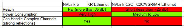
[3.a] Reach and Tradeoffs
As you can see in the spec, there are additional members of the alphabet soup such as “KR”, “LR”, “C2M”, and “VSR”. This is because Ethernet is divided up into sub-standards based on reach.


Analog (PHY/SerDes) designers can target one or more of these reach specs. For example, one PHY IP might support KR, LR, and C2M but cannot handle VSR. Another PHY (from the same company) can be designed to support C2M and VSR only.
There are power, area, and performance tradeoffs. PHYs designed for long reach will have larg DSP (digital signal processing) chains. Say around 40-80 FFE taps. Meanwhile, a short-reach Ethernet PHY may only have 15-30 FFE taps.
Many more changes can be made. I am giving you one vague (intentionally obfuscated) example.
NVLink C2C is analogous to a C2M or VSR style Ethernet SerDes. Short reach, lower power and small die area.
NVLink5 is analogous to a super KR style Ethernet SerDes. Ultra-long reach, large die area, guzzles power.
Let’s look at some snippets from official spec so you can get an intuitive understanding.
Note: IEEE 802.3 defines a standard package model of 4 dB insertion loss for both Tx and Rx. The bump to bump (realistic) loss is whatever the table says + 8 dB. Most people calibrate out the package via de-embedding. IEEE provides a “informative and unofficial” MATLAB script called the “COM” (channel operating margin) script that does this de-embedding. Everyone uses it.
KR (backplane) spec.

CRC (chip to chip) spec requires testing at different (lower) insertion loss.

There are 5-8 of these, depending on how you count.
Can one SerDes drive all of these channels in a power efficient, high-performance manner? No.
It is standard to make (at least) two SerDes. One for super long reach and lots of nasty reflections. Another for short reach for power sensitive applications.
[3.b] Why “Open” is not Neccisarily Better
The best way to explain this stance is with some examples.
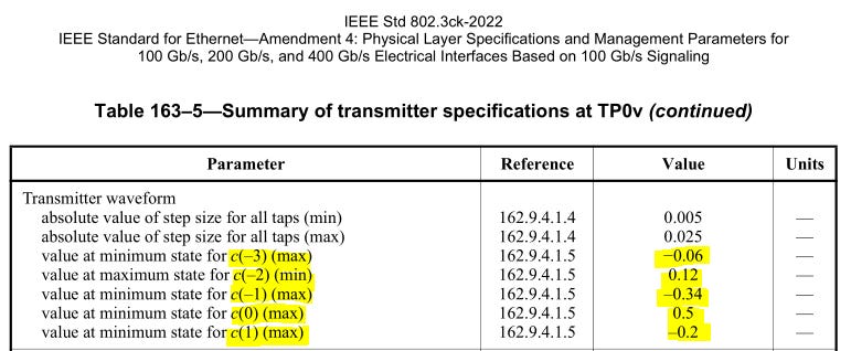
Ethernet transmitters have a 5-tap digital FIR filter. This digital pre-distortion filter allows for correcting of reflections and channel conditions, improving performance. When you plug in an Ethernet device (really any modern SerDes), the remote receiver requests different Tx FIR settings in a process called link training.
Because both sides need to agree on the possible configuration space ahead of time, rules must be set in place within the standard.
Maybe 7-tap FIR filter would help. You have to use 5 if you ar3e building for Ethernet. Maybe NVLink5 has more FIR taps to accommodate stronger reflections from the backplane. No idea.
Some rules make sense. For example, the absolute value of all the taps summed must be less than or equal to one. This makes sense as you don’t want to scale the signal at this stage as that would mess with analog transmitter specs.
What does not make sense as the artificial limits of each taps sign and strength. Why must C(1) and C(-1) be negative? Why limit the strength of the taps?
From digital filter theory, these limits seem pointless. Ask a group of SerDes engineers why these limits to Tx FIR exist and 95% of them won’t be able to give you an answer.
Every engineering standard has some dumb shit jammed into it. For Ethernet, look no further than “differential effective return loss”, dERL.
“Return loss” is a measure of how “reflective” a circuit is. Reflections are bad so you want this number to be low.
Traditionally, you measure ERL on a machine called a VNA and plot the s-parameters. There is some mask where you line has to stay under. Thats it. Easy.

Modern Ethernet requires dERL, a retarded, overcomplicated, nonsensical measurement where you have to feed s-parameters into a five-thousand line MATLAB script from hell such that it spits out a number nobody actually understands. Some dumbass at Intel came up with this joke of a measurement and shoved it into spec.
I hope Lip-Bu Tan fires him.


Finally, we have temperature ranges
Ethernet requires the PHY to operate anywhere from -40C to +125C die temp.
Yes, those numbers are really what is required.
The reason for such extreme temperature requirements is the Ethernet PHY might be in an industrial/automotive scenario. Say a hot factory with poor cooling or a cell tower in a snowy environment. Designing the PHY to perform well across this wide temperature range is not only difficult, it forces performance sacrifices.
Do you think Nvidia gives a shit if NVLink works at -40C? NO!
They designed the SerDes to work really well at 20-90C die temp probably as that is what can happen in a liquid cooled datacenter.
[3.c] Practical (Visual) Overview
Let’s look at the GB200 board and rack-scale NVL72 system to understand why NVLink5 and NVLink C2C are materially different even though both are 200Gbps SerDes.

As you can see, the distance between the CPU and GPU (covered by NVLink C2C) is rather short. More importantly, its just a PCB which means there are not many strong reflections.
Reflections require heavy DSP to correct. NVLink C2C (just like a VSR or C2M Ethernet PHY) can cut a lot of stuff to save power and die area.
NVLink5 has to deal with the now legendary Amphenol overpass cables and backplane. All you investors wondered why that shit has caused so many problems… hopefully now you understand.
REFLECTIONS! REFLECTIONS! REFLECTIONS!

REFLECTIONS! REFLECTIONS! REFLECTIONS!
Every connector adds a possibility for impedance mismatch and reflections. Fucks up the signal real quick. Testing so many connections at once has been a nightmare but innovative companies such as Multilane have developed a unique solution that is rapidly improving the manufacturing landscape.
[4] Strategic Impact
This move by Mr. Leather Jacket is truly galaxy-brain. It fucks over so many competitors. Truely glorious. Jensen is playing 420-dimentional chess as the Hypersaclers munch on checkers pieces and crayons.

NVLink Fusion re-shapes the entire AI ASIC landscape.
[4.a] Nvidia
This is a massive strategic win for Nvidia. Jensen has murdered UALink before it could be born. The lock-in from this NVLink Fusion program is incredible. Nvidia forces NVLink C2C PHY and MAC upon 3rd party chips, locking those designs into the Nvidia ecosystem. Important, differentiating IP (long-reach NVLink5) is protected by keeping it in a Nvidia-only Fusion chiplet they design, supply (via TSMC) and track.
Money is not the objective here. Even if Nvidia charges $100M in NRE for the NVLink C2C IP to 10 customers, that is only $1B in one-time revenue. Actually nothing in the grand scheme of things. $100M of NRE for a single IP block is a ridiculous number BTW. The actual prices are almost certainly much lower.
But then what of the Fusion chiplets? It’s a small die with high yield. Even if Nvidia charges 90% gross margins, the revenue will be small relative to Blackwell GPUs at 70-75% gross margins at MUCH HIGHER ASP.
Make no mistake, this is Nvidia trying to murder all competition except Broadcom. Brilliant long-term strategic move.

[4.b] Synopsys, Cadence, and Alphawave
All three of these companies lose in various severity. The IP departments of Synopsys and Cadence just got their TAM slashed as Nvidia is now directly competing with them using a completely superior 200G PHY.
Both Synopsys and Cadence will be fine as investments. The core EDA business is unaffected. The IP departments are kinda toasted. Some people are prob going to be fired.

Alphawave is in deep shit.
That Qualcomm acquisition offer is probably gona go BYE BYE. LOOOL.

[4.c] Broadcom
You may think this hurts Broadcom but I think NVLink Fusion is neutral at worst, probably a net benefit to Broadcom.
Nvidia is murdering several competitors who also compete with Broadcom. Thus, the market becomes a brutal duopoly/oligopoly where both sides print money and the customers have no choice but to pay.
[4.d] Alchip, Marvell, and Amazon
The Trainium 3 dumpster fire has been glorious entertainment.
First, Amazon pays NRE to both Alchip and Marvell for Trainum 3 under the same codename. Supply-chain degens go nuts arguing who got awarded this shit project before it becomes clear Taiwan buy-side is right and Alchip got it.
Then, Alchip fucks up integrating the Synopsys 200G SerDes and has to re-spin. Now rumor is Marvell got the Trn3 IO die even though their 200G SerDes is crap too.
Amazon is trying to figure out how to salvage this shitshow as both Alchip and Marvell join the NVLink Fusion program.
Marvell is now openly admitting their 200G SerDes is shit.

[4.e] Astera Labs
Asteral Labs is working on their own 200G SerDes because the Synopsys/Cadence/Alphawave 200G is not good enough. Currently, Astera Labs re-packages Synopsys SerDes. They know they need to make something better. Every port on their stuipd PCIe switch needs a fucking re-timer.
Now that you know why Astera Labs OpEx is blowing up, what happens to that R&D now that they have joined NVLink fusion? PCIe switch market just got a lot smaller.
[4.f] MediaTek and Google
If corporations are people, then Hock Tan has Google by the balls. It is well known within industry that Google has been DESPERATLY trying to find ANYONE with a viable 200G SerDes so they can design-out Broadcom. Google has pinged every single vendor multiple times over the past two years and nobody can meet their ridiculous post-FEC requirements. MediaTek has already failed once on N4P and is rumored to have failed again on N3P. According to a trusted contact in Taiwan, half the MediaTek SerDes team has left to join Nvidia recently.
Maybe they know they are doomed now that MediaTek has joined the NVLink Fusion program.

Mr. Leather Jacket seems to have killed MediaTek’s 200G SerDes team and forced Google back to Broadcom or into NVLink Fusion.

[4.g] Fujitsu and Qualcomm
The vanilla V2 ARM IP CPU cores in Nvidia Grace are crap. Fujitsu and Qualcomm are making custom ARM-compliant CPU cores that will go into a server product. NVLink Fusion is a great win for both. Instant access to a very large market that commands higher margins than the cloud-native cheapo CSS chiplets ARM makes for the Hyperscaler internal CPU workloads.
I hate to say it but this is… good… for Qualcomm.
(very funny though… Qualcomm execs hate Nvidia)
[4.h] AMD and Other UALink **LOSERS**
UALink is an AMD specification that they donated to the consortium. Early UALink draft specs said “AMD CONFIDENTIAL UNDER NDA” in big bold letters and the top of each page alongside the AMD logo. Subtle.
Jensen has brutally murdered UALink like that one scene from “Game of Thrones”.
You remember... the red wedding.”
AMD was already in deep shit because UALink switches were super far out. Most likely 2027 volume ramp. Semianalysis has highlighted this problem several times.
Who is going to want to develop UALink switches now? Astera Labs has already defected to NVLink fusion. Are the random crypto miner losers turned AI switch vendors gona help AMD defeat Nvidia Vera-Rubin? LOOOOOL
Everyone associated with UALink is a NVLink fusion loser.

The “L” in “UALink” stands for “LOSER”.
L
O
S
E
R
Weren't you impressed with MediaTek's SerDes? Is the probability of success for TPU V7E very low now?
https://irrationalanalysis.substack.com/p/isscc-2025-ultra-high-speed-serdes
I may not be smart enough to understand, but I want more clarity.
They're licensing NVLink C2C, right? But what's the benefit for companies with custom ASICs and why would they use it? Access to Grace CPU or NVLink 5? AFAIK the first is kind of meh. The second is cool, but why would they go for NVLink 5 instead of what they use now (I assume Broadcom)?