
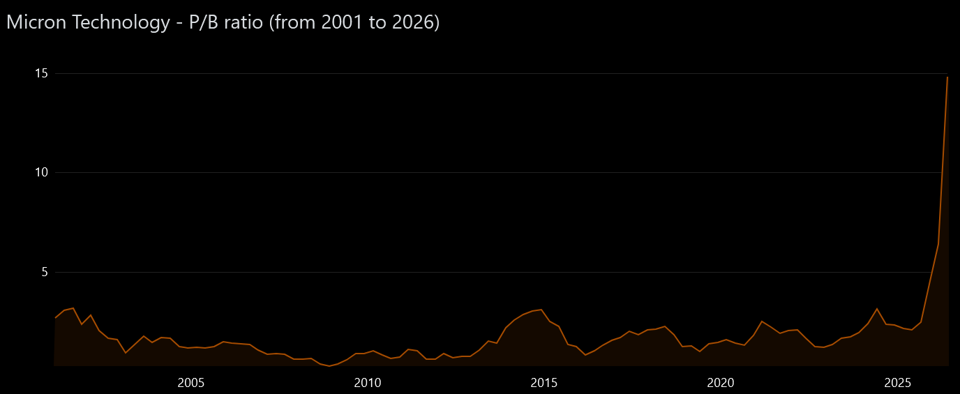
HBM: High-Bandwidth Mistake
Updated views on DRAM.

Irrational Analysis is heavily invested in the semiconductor industry.
Positions will change over time and are regularly updated.
Opinions are authors own and do not represent past, present, and/or future employers.
All content published on this newsletter is based on public information and independent research conducted since 2011.
This newsletter is not financial advice and readers should always do their own research before investing in any security.
Feel free to contact me via email at: irrational_analysis@proton.me
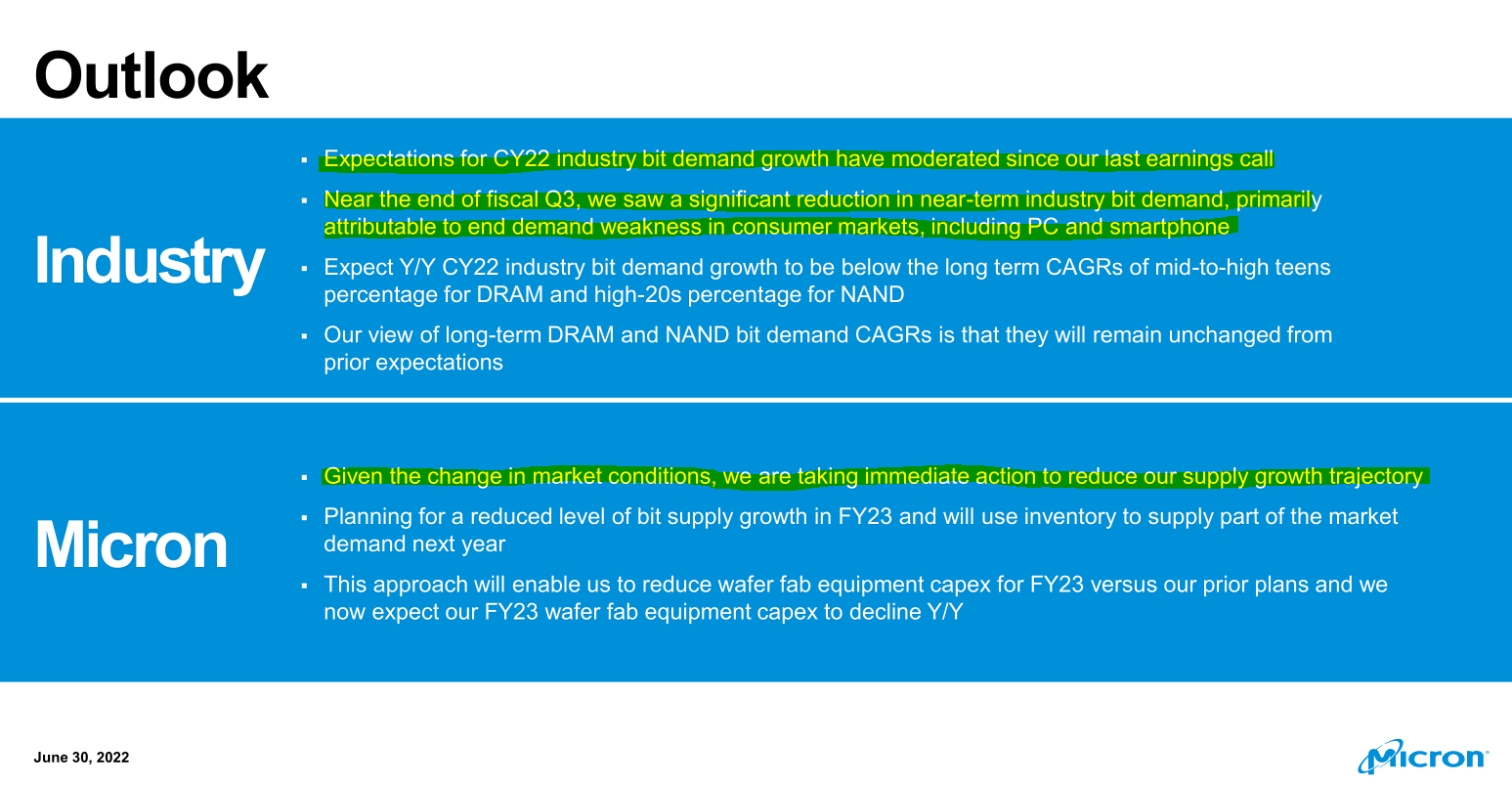
Welcome to an updated view (partial capitulation) on memory. Specifically DRAM. Nand/flash is outside the scope of this post. Go away Sandisk bulls.
I have been negative on DRAM (Micron/Samsung/SK) as an investment due to persistent fears of cyclicality.
There are two camps:
Team price/book
Team price/earnings
Each side thinks the other is completely retarded.
Still consider myself in team price/book but… willing to make an exception and consort with the other side temporarily.
Funny story….
Two years ago at GTC 2024, I was at one of the after-parties waiting to meet Doug for the first time in real life. At the party, Dylan and a few random hedge fund people were chatting. One of the hedgies was talking about how his PM/boss said “if you see a bubble forming, run towards it”.
*This quote is from George Soros. Random hedgie minion def does not work for Soros so he mis-attributed the quote.
Spicy Takes:
I believe HBM is a mistake and will be phased out (90% drop in volume from peak) within the next 7-10 years.
DRAM stocks prob have another double or triple left in them.
At some point in the next 3-10 years, DRAM stocks will drawdown at least 70% from peak.
Contents:
Engineering
HBM is a mistake.
[short term] Hybrid-bonded HBM is necessary.
[partial solution] CXL
The optimal (future) approach.
Entertaining History
Agentic Reality: Featuring Nick/Coatue
Pitch: Samsung
[1] Engineering
Let’s start with engineering topics. Some level of background is needed.
Memory is in two categories:
DRAM
NAND aka Flash aka NAND Flash
Within DRAM, there is DDR, LPDDR, GDDR, and HBM. I view all of them as equivalent and you will see why shortly.
DRAM, NAND, and logic all have separate process technologies. The factory capacity is not fungible.
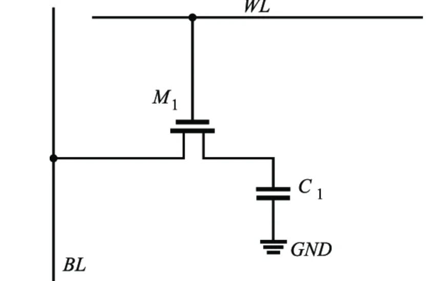
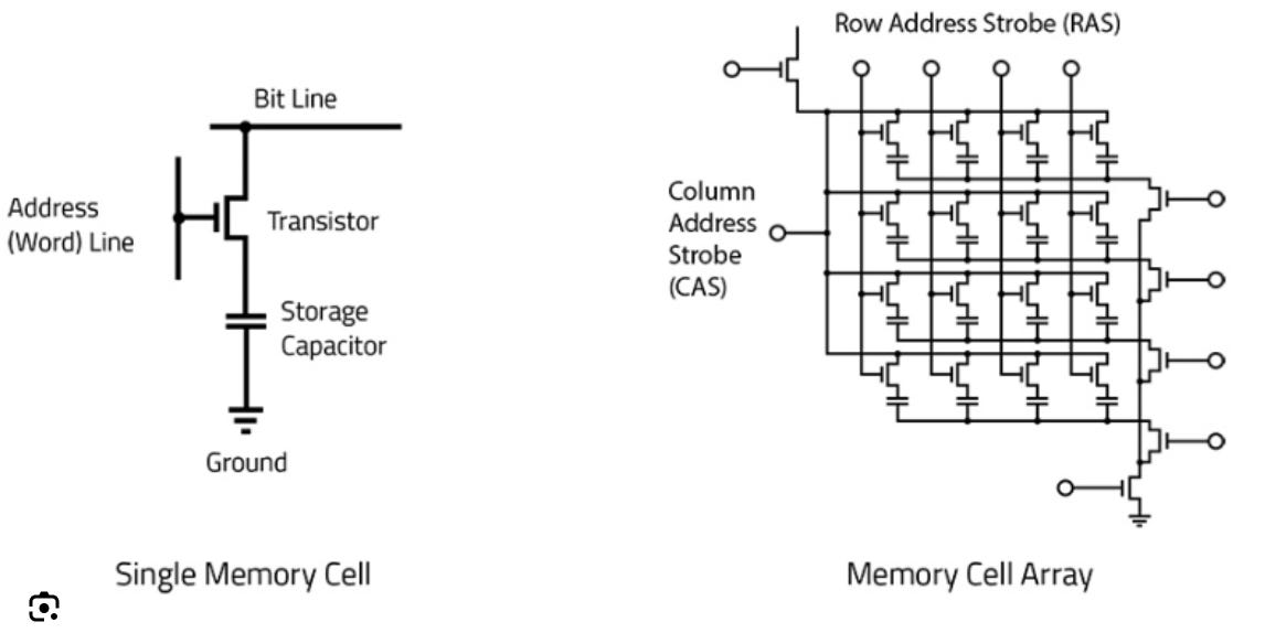
All DRAM works the same in principal. A transistor controls the charge of a capacitor. Reading the bit drains the capacitor. The capacitor also naturally loses charge over time so it constantly needs to be refreshed. This is why DRAM is referred to as volatile memory, it needs power to store data.
DRAM has only four core attributes:
Latency
Bandwidth
Capacity
Power Consumption
Changing the structure of the grid of capacitors and transistors gives you DDR vs LPDDR vs GDDR but it really is all the same at a high level.
HBM is different because there is vertical stacking.
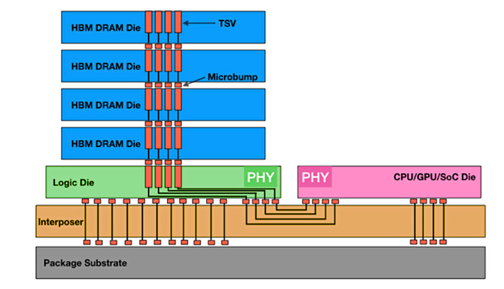
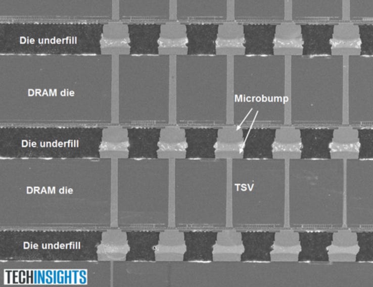
Some of the DRAM die area is occupied by TSVs (through silicon vias), vertical wires.
There are also micro-bumps to connect the dies together.
HBM (high-bandwidth memory) gives you high-bandwidth, but at a high cost. This cost (economic, thermal, power) is going up at an untenable pace.
Don’t believe me? Take a look at the Rubin HBM4 fiasco.
JEDEC is the standards body that governs DRAM. Generally, when a new spec comes out (DDR5, LPDDR5X, HBM4, whatever) there is an initial speed agreed to in spec and over time industry adopts higher speeds over time.
With HBM4, JEDEC spec said 8 Gbps/pin and immediately Nvidia Rubin (first product to ramp) demanded 11 Gbps/pin. All three major HBM vendors (SK Hynix, Samsung, Micron) proceeded to fail to meet this request at various severities. Endless drama from the supply-chain leaker degenerates.
The root cause of this fiasco is simple. Bump capacitance. Will get to that in a later section.
HBM4 rollout is an industry-wide fiasco.
JEDEC are idiots for releasing a spec that is immediately obsolete.
All the consumers of HBM4 look like fools for making last-minute demands that cause chaos and delay their own roadmaps.
All the HBM vendors look stupid for claiming they can meet 11 Gbps or 10 Gbps then failing Nvidia qualification process because none of them know how to use high-speed probe stations.
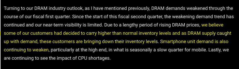
[Market Memo] Tower+GloFo Earnings, HBM4 Qualification Noise
![[Market Memo] Tower+GloFo Earnings, HBM4 Qualification Noise](https://substackcdn.com/image/fetch/$s_!jFo9!,w_1300,h_650,c_fill,f_webp,q_auto:good,fl_progressive:steep,g_auto/https%3A%2F%2Fsubstack-post-media.s3.amazonaws.com%2Fpublic%2Fimages%2F246b0900-766d-48ab-846f-bbe5c5daf35b_869x686.png)
Irrational Analysis is heavily invested in the semiconductor industry.
[1.a] HBM is a mistake.
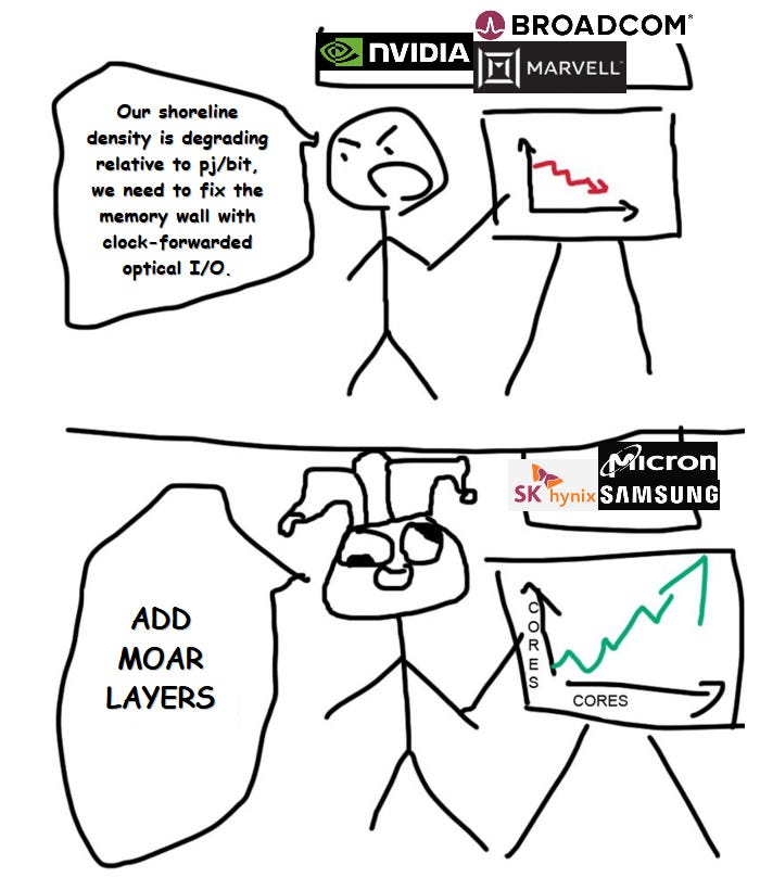
Memory bandwidth is an I/O density problem which has been solved in the wrong way by the wrong people.
You see, 11 Gbps pin speed is still… shit compared to everything else on the market outside of DRAM-land. 32G short-reach SerDes (UCIe AP, NVLink D2D, Marvell D2D, Broadcom MAX) are ubiquitous. Hell the 64G class versions are either already in prod or close.
DRAM crowd was given a PHY problem and botched it. Now, other companies are making custom solutions to bypass the fail. See this example from Marvell.
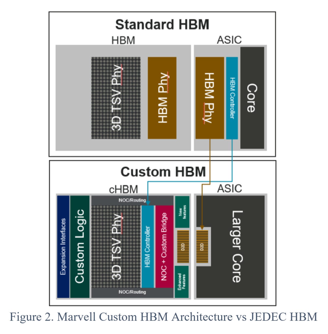
Diagram is not to scale and just illustrative but the point is clear. If you don’t use a retarded PHY, you can save a lot of ASIC shoreline and shove more of them in. Orange box gets smaller.
In this case, beachfront width does not improve because the TSVs of the HBM still limit even though the custom Marvell PHY is way better.
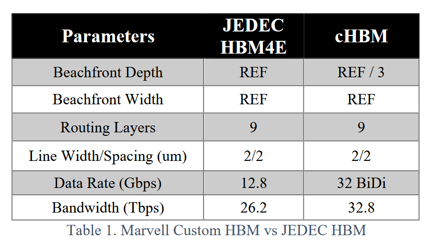
There are gains to be had from custom HBM base die. Marvell claims 25% more bandwidth. Great… but people want way more. AI is insanely memory bandwidth bound.
Key Points:
HBM PHY is dogshit.
Custom HBM base die partially mitigates this issue.
The TSVs are the real limit, locking up precious shoreline.
There are a variety of startups trying to solve this memory bandwidth issue. Some go for SRAM-heavy designs. Others use exotic processes. There is one startup that is my favorite and that is Positron. They solved this problem the “correct” way.
Unfortunately under NDA so can only give vague info that Thomas already shared publicly.
Positron does not use any HBM.
Only use commodity LPDDR5X.
Highest memory bandwidth of any AI ASIC.
Some clever architectural tricks to actually use all that bandwidth effectively.
Also know everything about Etched but under NDA. Architecture is very cool but they still suffer the same HBM limits as everyone else. Hopefully in the next few months I can negotiate proper coverage.
Positron gave me all their slides. Etched showed me the material but still wont send the PDF. MatX wont give me anything so IDK maybe I need to threaten them. Those Pope podcasts are useless and have zero real information.
Positron is the only startup that has properly addressed the memory bottleneck in my opinion. There is a better way that involves optics but in the short term, Positron’s approach is optimal.
[1.b] [short term] Hybrid-bonded HBM is necessary.
The HBM4 fiasco was driven by two primary factors, base die and pump capacitance.
Samsung used their internal SRF4X logic node (perf ~TSMC N6/N7P) and had the easiest time. Enough margin from the transistor performance to fix issues quickly.
SK Hynix chose TSMC N12 and… had like 6 re-spins.
Micron went full retard and tried to stay on internal DRAM process node for base die.

But even with a good base die, there is still the parasitic bump capacitance issue.
Let’s look at some squiggly lines!
This is a TDR trace (time domain reflectometer):
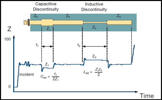
You can use a machine to map out the impedance of a system. Stare at enough of these squiggly lines and it becomes second nature to spot what part of the system made what part of the plot.
Probe a HBM stack (without the base die) and you will get a TDR trace with one spike per layer. The spikes correspond to parasitic bump capacitance.
Only way to (properly) fix this is to move to hybrid bonding.
Everyone keeps viewing hybrid-bonded HBM from a thermal or stack height perspective… which is valid.
My point is speed/performance is the real gate and what will finally push DRAM vendors to suck it up and use hybrid bonding.
Think of capacitors as speed bumps. You can make the base die as amazing as possible but those parasitic capacitors in the stack will kill your signal. Either blow up PHY power or accept lower speed.
Speaking of which… this SK Hynix innovation is more evidence HBM is a mistake.
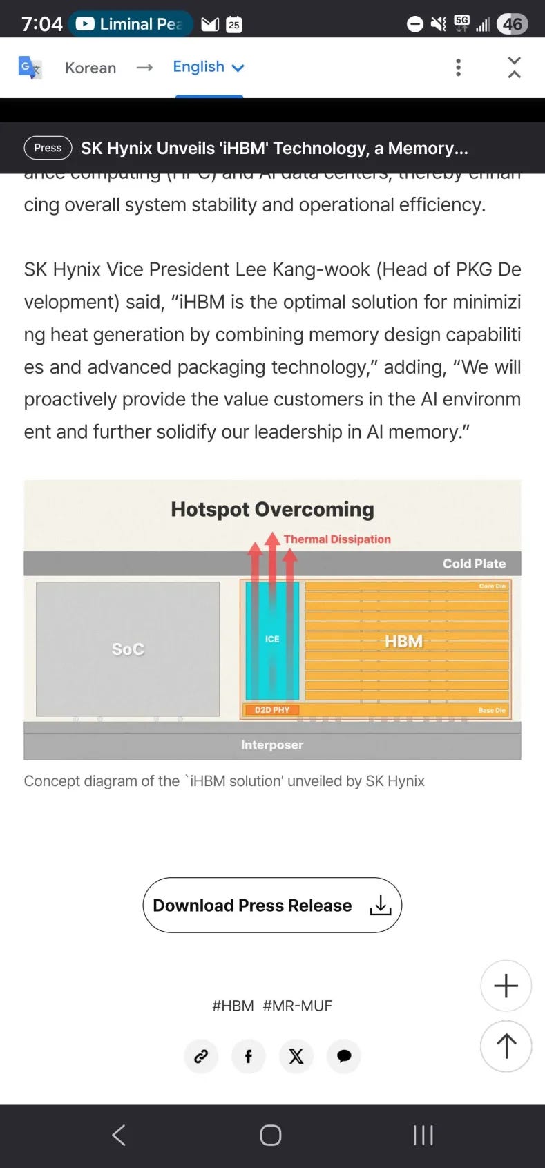
Why yes, the PHY power is gona blow up as speeds go up. Your solution is to have an overhang and place a thermal conductor pillar.
This is like trying to eat while wrapping your arm behind your head. Technically possible but stupid.
HBM is a mistake. The solution is to disaggregate memory with a real PHY that drives co-packaged optics.
[1.c] [partial solution] CXL
CXL is a protocol built on top of PCIe that allows for memory expansion and pooling. Initially designed for CPUs, it was abandoned. Now it’s coming back.
Great for Marvell and Astera Labs.
But still does not solve the problem properly. Remember, we have a PHY problem and CXL is just a protocol built on top of a sub-optimal PCIe PHY.
[1.d] The optimal (future) approach.
At ISSCC 2026, Nvidia showed a glimpse of the future. The correct approach to I/O beachfront problem, and by extension the memory bandwidth problem.
Clock-forwarded SerDes directly driving optics.

On the ASIC side, you have essentially no latency added to the system as there is no re-timer or need for a heavy (latency inducing) FEC. Shoreline density of clock-forwarded XSR SerDes is very high. Optics enable reach from 1 to 30 meter easily, once you go through the pain and suffering of getting the data on the optical fiber.
Clock forwarding allows for the entire Rx EQ to be gutted. No CDR, FFE, DFE, MLSE, or compound CTLE. Just a simple TIA.
Sub 3 pj/bit, up to 10 meter reach easily. More likely 30 meter should work assuming chromatic dispersion does not mess with the delay compensation circuitry.
Shoreline density is not great and you need to look at the die shot to see why.
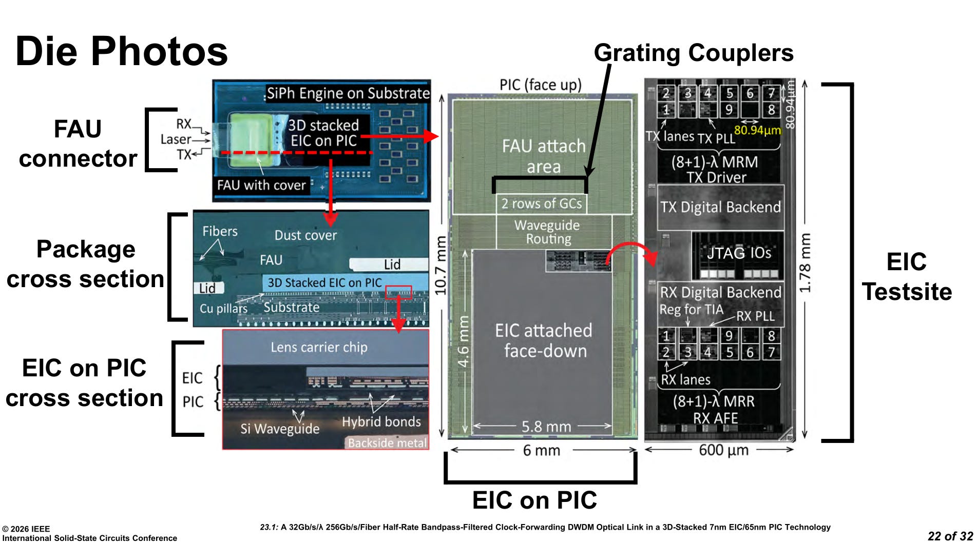
Each lane is in an 81 micron square. The Tx/Rx PLLs are the same size as an entire lane AFE. This does not make sense from an electronics perspective. My guess is photonic issues, particularly thermal crosstalk, forced the EIC to blow up in area. You can see the digital backend and JTAG separating Tx and Rx AFE. This was likely intentional to isolate ring modulator self-heating from Tx rings polluting Rx rings. Point is, the end state of this technology at commercialization is (well… should) going to be way better than 0.4 Tbps/mm unidirectional.
Because the system is optical, you can just route with an OCS that also has effectively no latency when compared to a traditional electrical switch.
On the device side, all you need is a chip that converts optical back to electrical (minimal latency) followed by some LPDDR PHYs. The latency will be dominated by the LPDDR PHY and controller. Perhaps clever optimizations will be enough. Perhaps a stack of HBM somewhere in the system used as a cache will be needed.
But this is the future in my opinion. Optically attached, disaggregated LPPDR memory pools. Nvidia is 2-3 years away from implementing this at scale. Broadcom and Marvell 3-5 years.
The benefits are enormous. Way higher bandwidth/mm shoreline density. Way more capacity. Minor latency penalty if done right. And most importantly, the ability to re-use and re-allocate DRAM across chips instead of packaging them forever with the ASIC while also enabling the ASIC to draw more power due to higher thermal headroom.

It get’s even better. You probably have heard of the HBM trade ratio. How many GB of regular DRAM capacity is consumed to produce 1 GB of HBM.
It is like 3:1 or something. The actual number does not matter. Its a big number. Massive supply destruction has HBM mix goes up.
If that reverses, you would think the DRAM vendors would get screwed but I disagree.
Right now, they are making 80% ish gross margins. At that profitability, all the customers know they are getting screwed and are thus unhappy and strongly incentivized to find a way out.
Imagine a world where HBM is replaced by LPDDR, DRAM supply is 3x, gross margins go down from 80% to 60%.
Everyone wins in this scenario.
DRAM makers end up with 2.25X profits (do the math retards) with 3x revenue at modest margin cut while also not pissing off all the customers.
DRAM customers get 3x supply at much more palatable prices to satisfy insatiable agentic AI demand.
DRAM customers also don’t have to worry about advanced packaging yield as much and can scale their logic chips more instead of wasting space on HBM stacks.
[2] Entertaining History
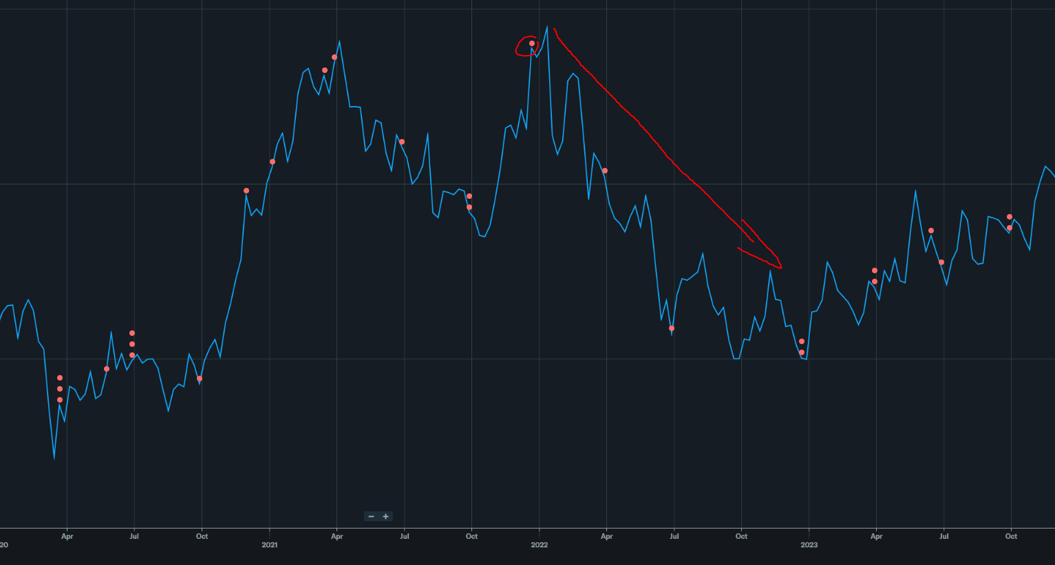
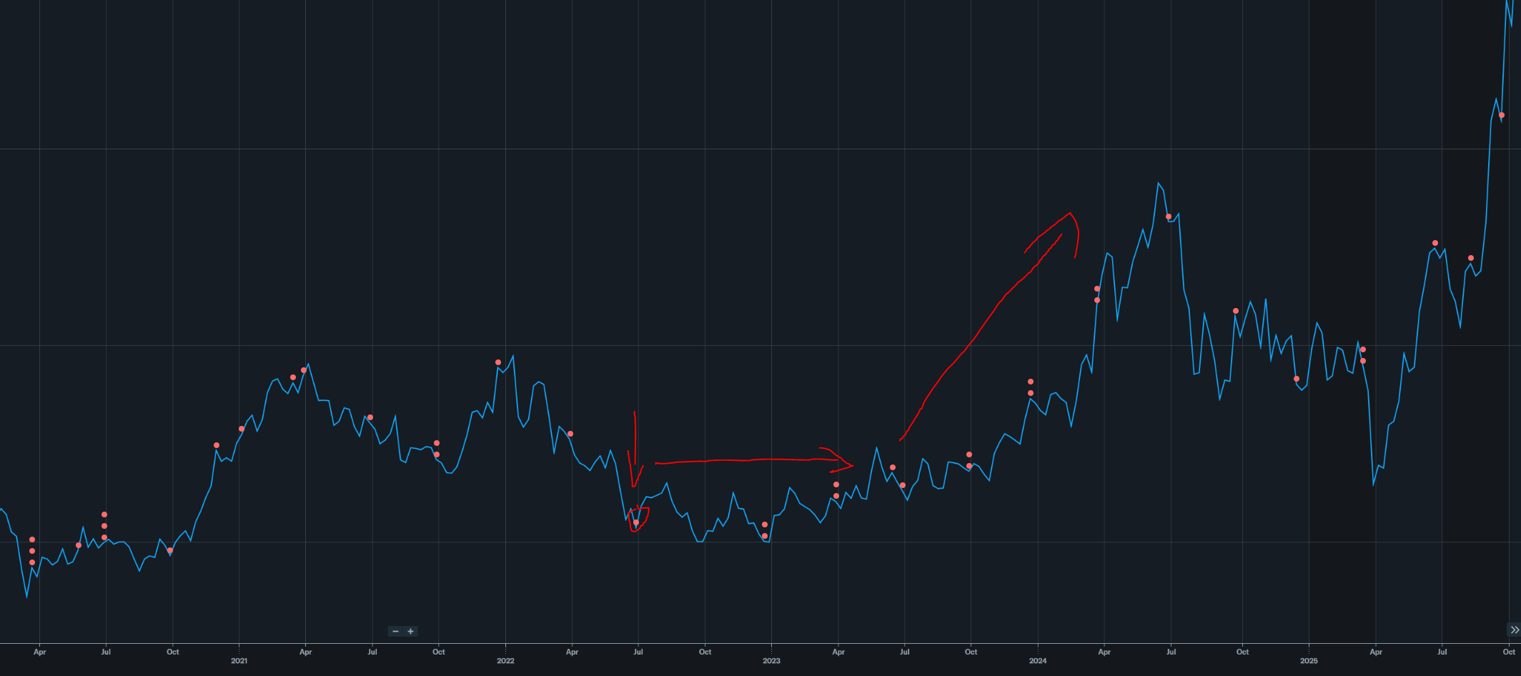
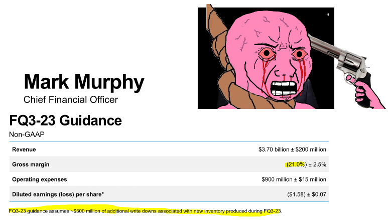
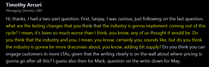
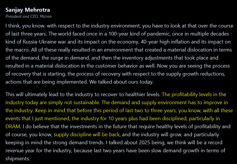
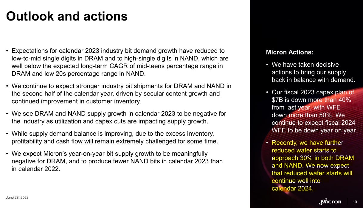
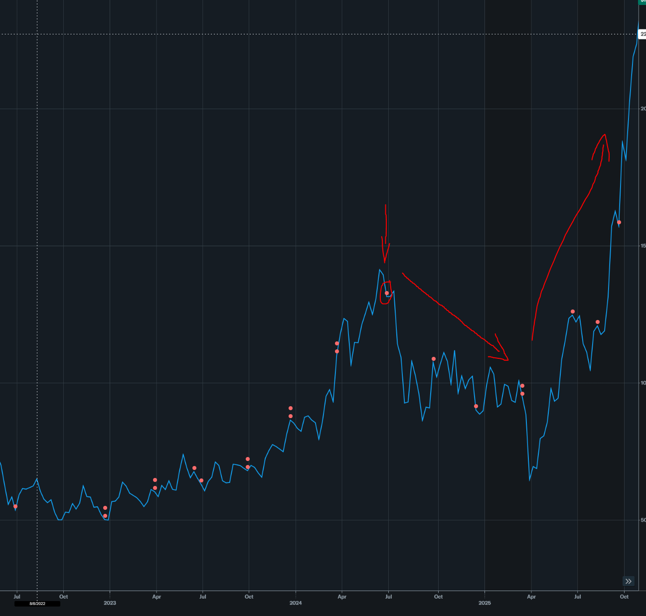
To understand the history of DRAM companies, you must read the transcripts of past earnings calls. This is typically a boring process so to keep people interested, I will roast Sanjay Mehrotra (Micron CEO) for entertainment purposes. There is a particular feature of Micron earnings decks that makes this goal easier to achieve.
We are going to look at every earnings call transcript from June 2017 (first call with Sanjay as CEO) to June 2025, the last earnings call where a negative dip happened before the crazy rally started.
You really should read this section in it’s entirety. It’s important.
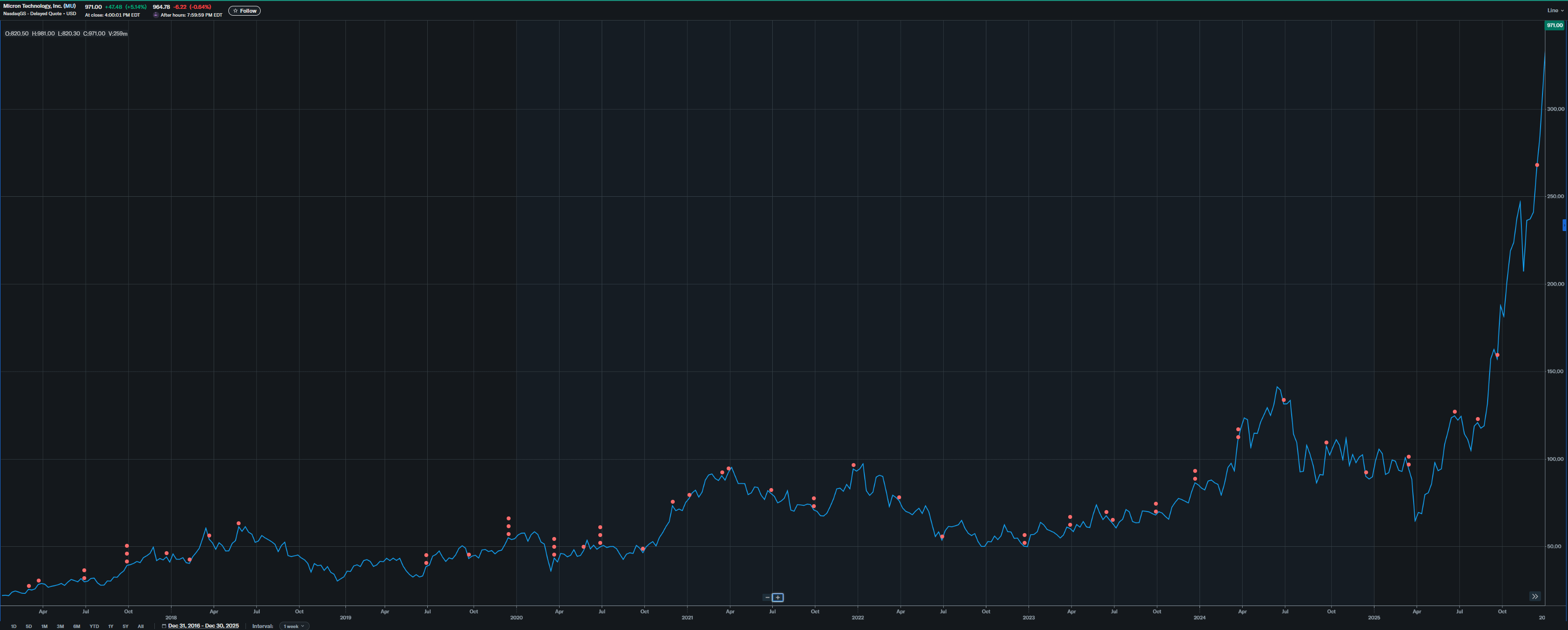
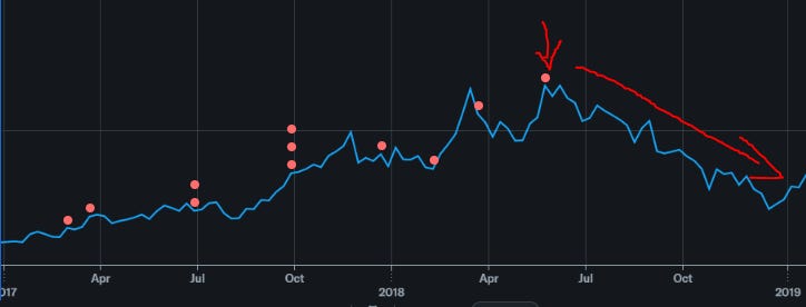
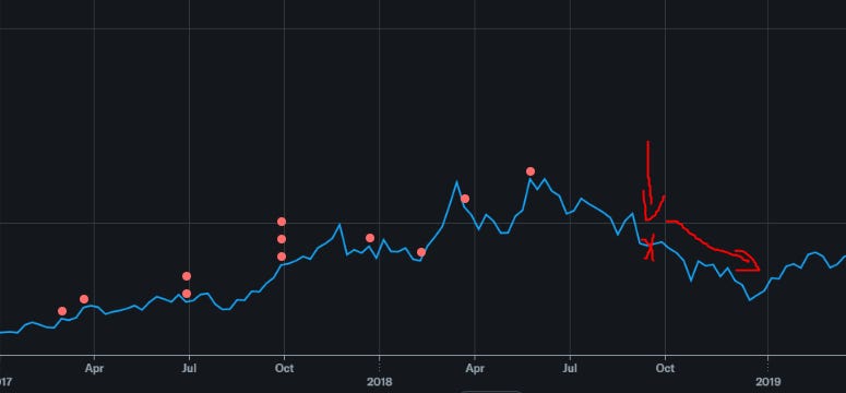
June 2017: $30/share
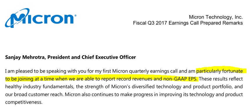
Sanjay did time his join date of March 2017 well. It was at the bottom of the cycle. 2017 cycle was particularly nice for the DRAM players. I remember as I was in college trying to buy DRAM for a gaming PC build. Fucking DDR tripled in price or some shit.
Sept 2017: $39/share
Ah yes, strategic value, not a commodity. Yes Sanjay pump your RSU.
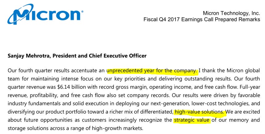
Dec 2017: $43/share
One of the biggest red flags you can see is mentioning cost competitiveness in one sentence then literally mentioning high-value in the next sentence. It is a sign of someone who knows he is selling a commodity but wants to pretend otherwise.
Mar 2018: $57/share
Well buddy the cycle is about to turn so I hope you got some of those high-value solutions to insulate you.
June 2018: $60/share (TOP OF CYCLE)
Ah yes starting buybacks at the top. Great start.
This time is different guys. Stability in the market!
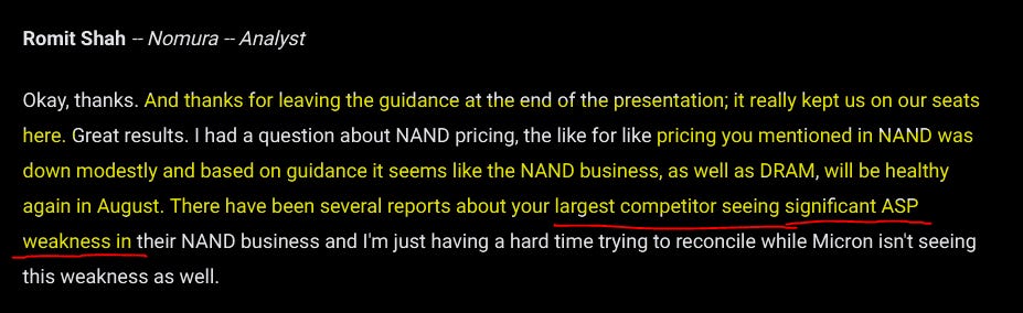
You can see the Nomura analyst shitting on Micron management. Thanks for keeping important negative guidance info at the end of the presentation you little shits.
Guys it’s just a 1-quarter blip. Next quarter prices will be healthy again. This is def not peak cycle and we certainty are not gona crash.
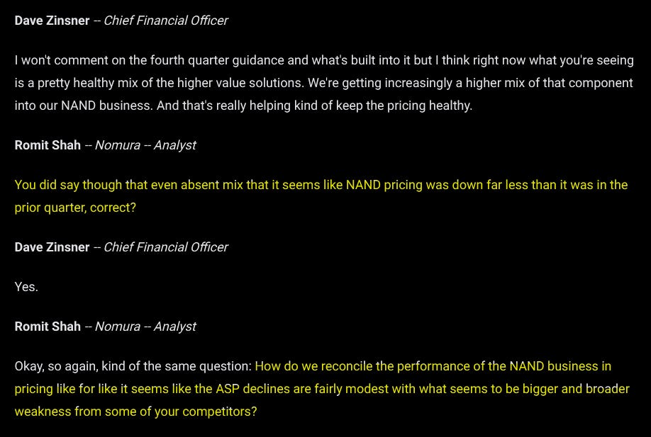

Are your gross margins deteriorating because of price cuts (very bad) or mix shift (ok excuse).
Hint: it was because of price cuts. OVERSUPPLY BAYBEEEE.
Analyst: Is this cycle (2017-2018) different this time?
Sanjay: Yes.
(it was not different that time)
Sept 2018: $45/share

Sounds like youssa in a down-cycle.
Dec 2018: $32/share (CYCLE BOTTOM)
Oh look this time was not different! Youssa eating shit in downcycle and resorting to decisive (desperate) actions.
Datacenter NAND/SSD is going to be great for us.
Also we are going to eat shit in this exact segment for the next year.
O V E R S U P P L Y
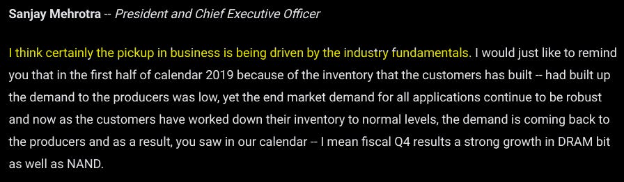
June 2019: $42/share
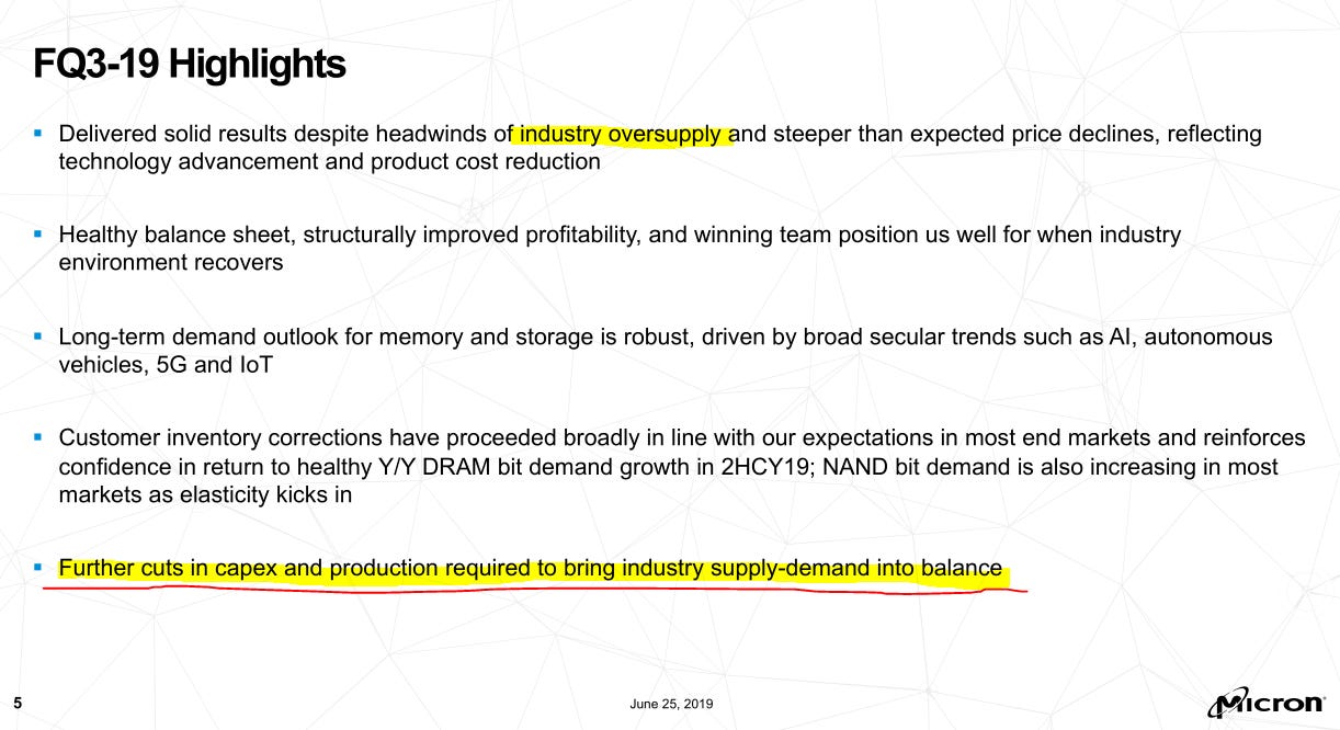
Ah yes you finally said the dirty word.
OVERSUPPLY
We made it past the usual euphemism of “inventory adjustment/digestion”.
The last sentence is a public call for Sanjay’s degen Korean friends to have mercy.
Sept 2019: $46/share
Amusingly this was probably true… and only a few months later COVID lockdowns hit right after inventory over-stocking due to tariff fears.
Dec 2019: $56/share (local* top in upcycle)
*due to pandemic. Under other circumstances upcycle would have continued prob another 12-18 months cleanly.
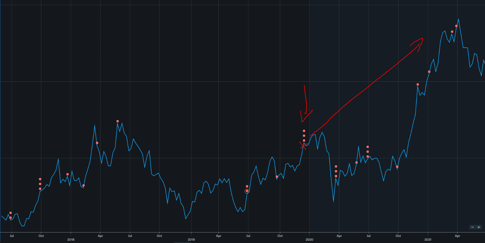
Stocks are forward looking. Smart people (not me lol) predicted when the bottom would be in and bought 6-8 months before Sanjay said the above quote.
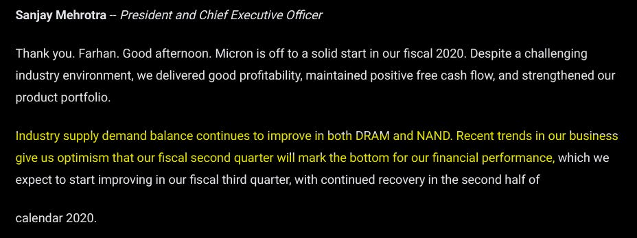
Mar 2020: $44/share
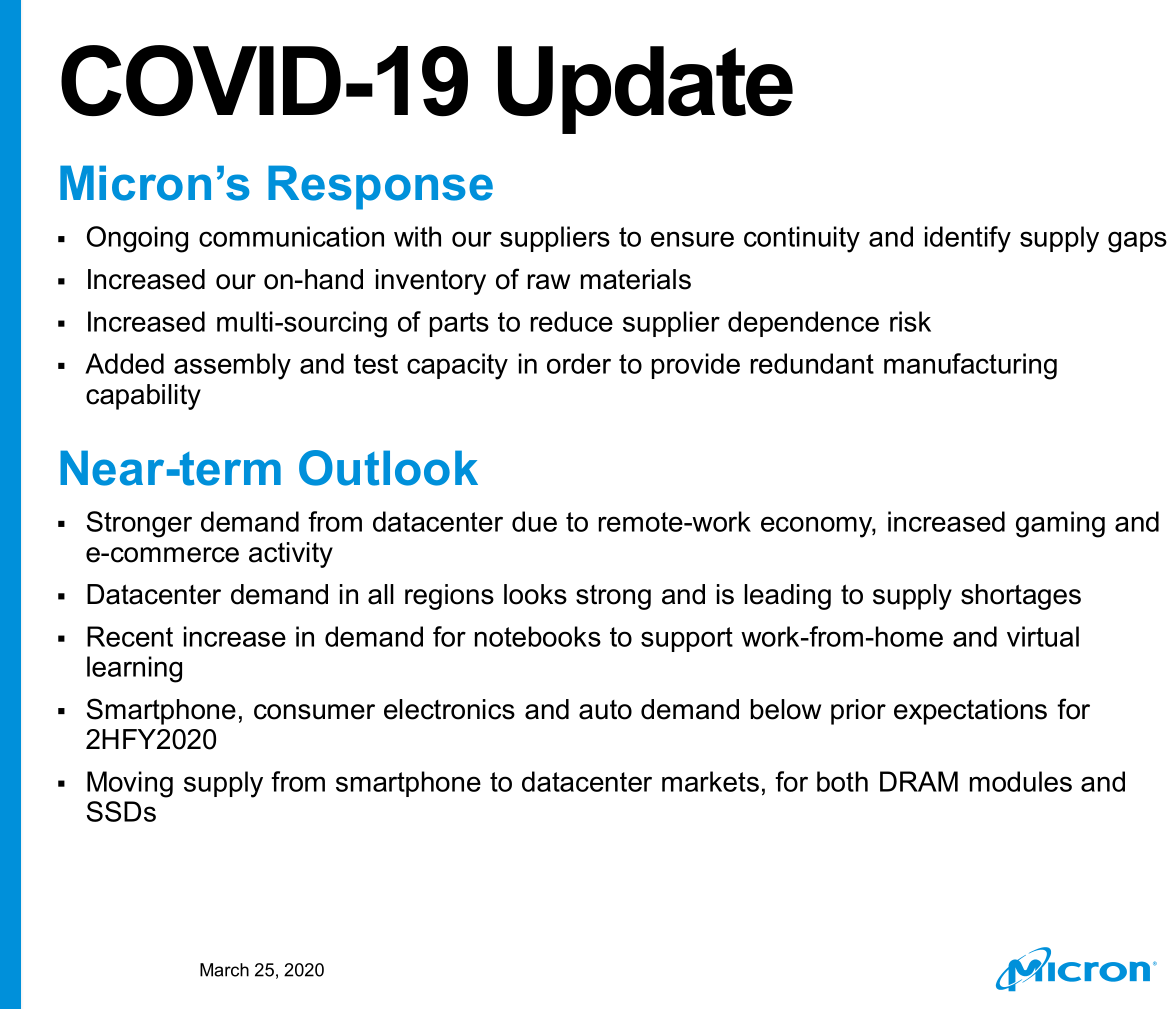
The next few quarters will be skipped because COVID bullshit distorts everything. All you need to know is the following events roughly played out:
Collapse in demand at the beginning (fear)
Then an explosion of demand because work-from-home, bored people, stimulus checks. (the “COVID pull-forward”)
Let’s skip ahead 9 months to happy Sanjay riding the COVID consumer electronics pull-forward wave.
Jan 2021: $78/share
Mar 2021: $92/share (CYCLE 1st TOP)
This is true. COVID pull-forward did hit all sectors same time.
Jun 2021: $81/share
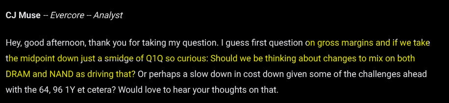
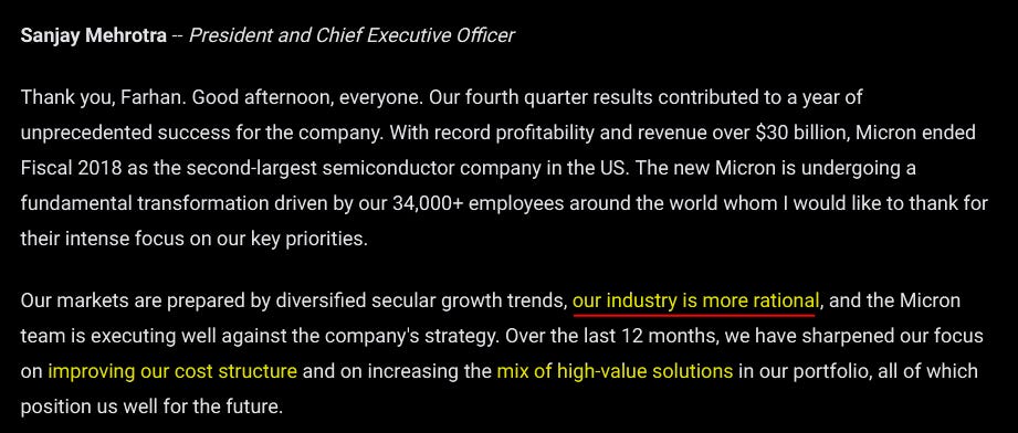
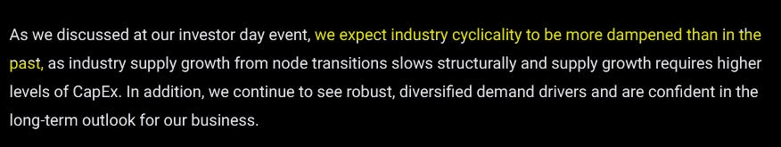
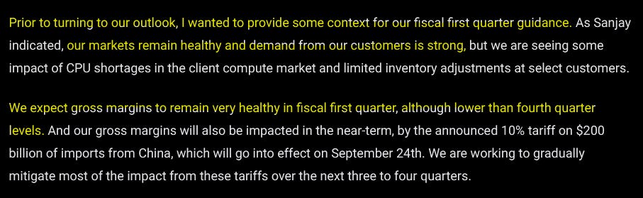
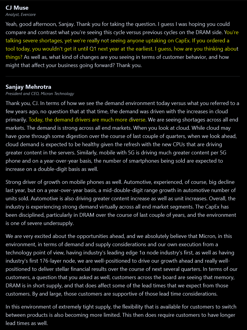
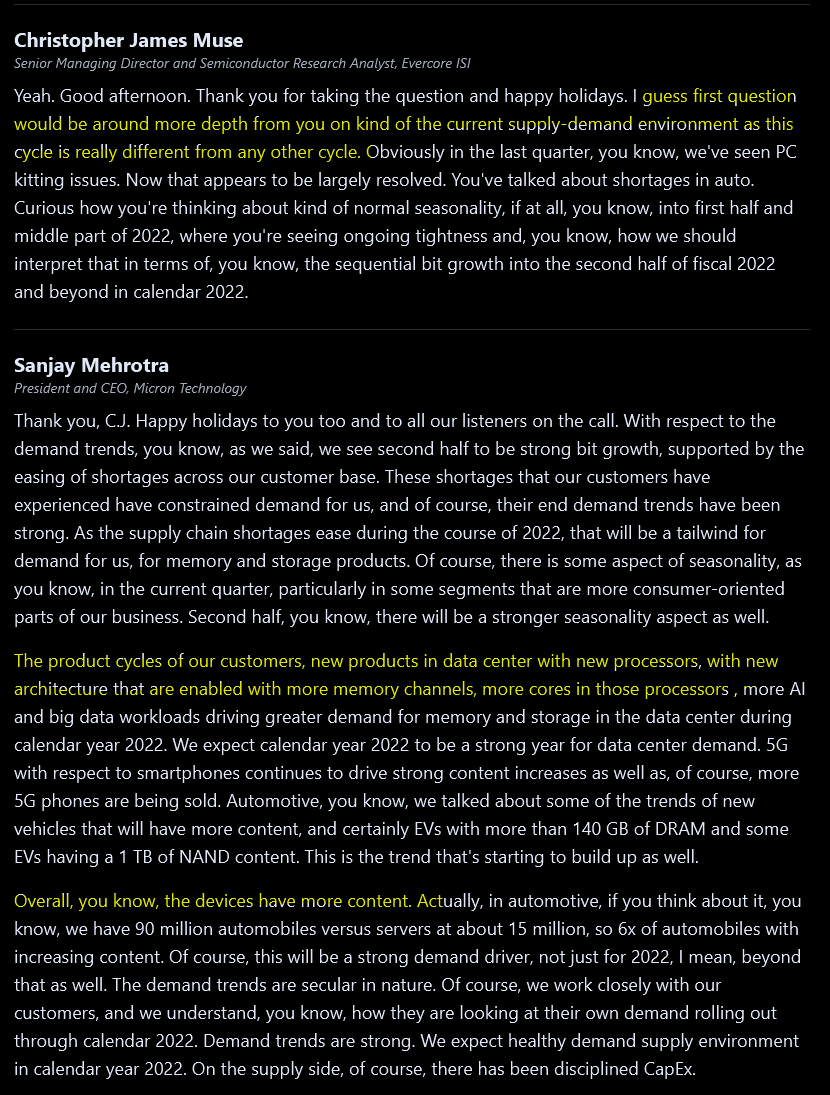
C. J. Muse is (correctly) pointing out that some bad omens are out there and Sanjay literally takes the opposite stance. Nonono demand for memory gona go up even more! Nothing unsettling to see here.
Joe Moore also smells blood. He is re-asking C. J. Muse question in a more subtle way to try and pin down Sanjay.
Sep 2021: $71/share (miD-cycle local bottom)
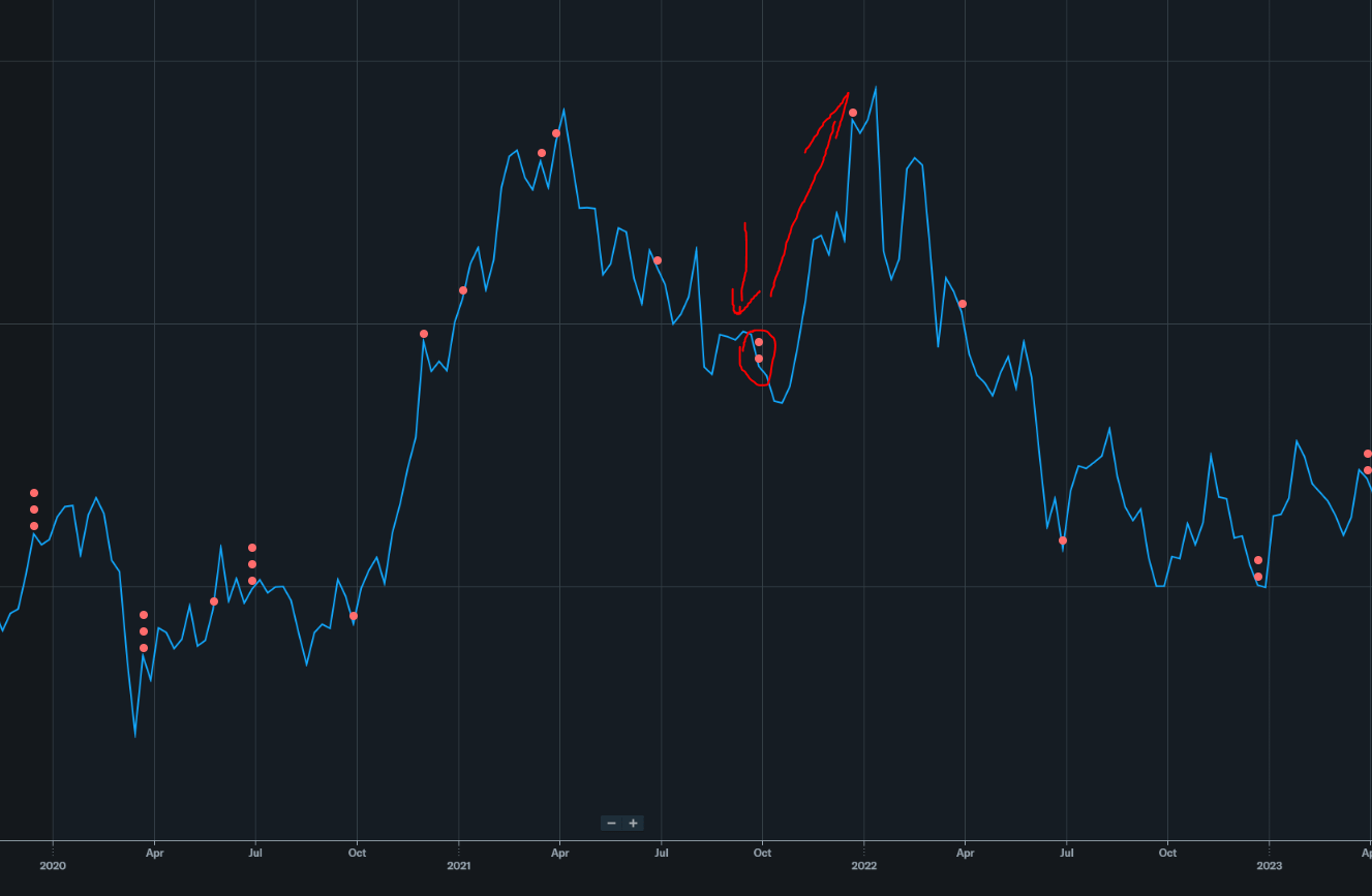
Again, the specter of over-supply (driven by COVID PC demand pull-forward) comes up.
Dec 2021: $94/share (CYCLE TOP)

I like to imagine Sanjay smoking a Cuban cigar during this call. Next two years are not gona be fun. Well not fun for him. Hilarious to me.
(PC would continue to implode lol)
You can C.J. Muse trying to warn everyone and Sanjay spouting bullshit.

Mar 2022: $78/share
Everything is fine guys. Nothing to see here.

As an aside, Zinsner got out at the right time. Good for him.
Jun 2022: $56/share
Not quite the bottom but getting there.
Oh so sell-side was correct three months ago and Sanjay was still off in la-la land?
You clowns told everyone PC was fine 90 days ago. Oh no its just chromebooks blah blah enterprise PC great. Idiots.
Slashing wafer starts. Let the panic begin!
Sept 2022: $50/share
Oh would you look at that, Krish Sankar of Sell-Side was correct that datacenter would be next shoe to drop. I guess Sumit Sadana is either incompetent or knowingly spouted bullshit 90 days ago.
Translation: we about to party like it’s 2001. Yea, that bad.
COVID pull-forward is finally hitting hard the other direction.
UNDERUTILIZATION LEZ GOOOOO

Mid-single digit utilization cut. Remember this number.
(Hint: it’s going up)
Vivek calling bullshit and Sanjay has to back-off rosy language on PC.
This is the key passage. Samsung is not cutting expansion plans. Everyone knows this. Micron is trying to avoid talking about this but the assumptions of their own guidance have Samsung expansion baked in.
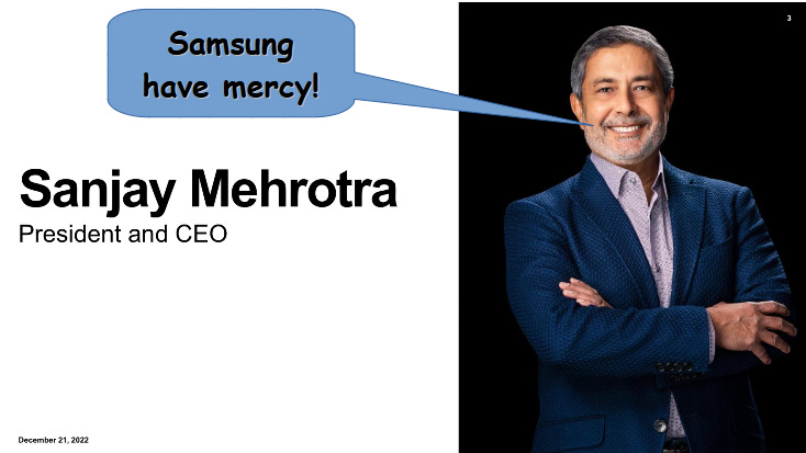
Dec 2022: $51/share (CYCLE BOTTOM)
Ok… 90 days ago you said on the last earnings call wafer starts cut mid single digits. Now that is up to 20% LOL.
Samsung is not cutting at all. This was at the low-point for Samsung Logic Foundry so the Device Solutions group was extra degen trying to gain share in DRAM to make up for logic failures.

Well at least he gave a straight answer. Kudos for that.
Mar 2023: $61/share
For those of you wondering why the DRAM vendors have not taken Hyperscaler offers for assisted CapEx, this is why. They nearly killed each other ~3 years go.
Sanjay is well aware that Samsung is the reason supply discipline has been fucked for last 2-3 years.
Jun 2023: $67/share
Well we started at mid single digit and now at 30% wafer start cut LOL.
Remember though stocks are forward looking. Micron already bottomed six months ago.
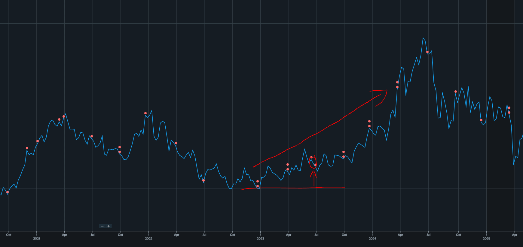
Sept 2023: $70/share
Still guiding for negative gross margins but remember stonks are forward looking.
Dec 2023: $86/share
Trending in right direction.
Mar 2024: $114/share
Back to good utilization and HBM trade ratio starting to destroy supply.
The trade ratio stuff was correct but there is one more dip before Valhalla.
Jun 2024: $133/share (local top, driven by HBM hopium)
Micron made a lot of noise about their HBM3e but it turned out to disappoint finance crowd.
The correction back to ~100/share was due to missed HBM3e expectations. Then we had liberation day that liberated my portfolio from gains. Then DRAM went vertical.
Sept 2024: $107/share
In truth I am tired so gona finished off this section half assed. There was some noise on Micron HBM3e qualification then even more noise on HBM4 qualification but in the end none of it mattered. Moon bitches.
[3] Agentic Reality: Featuring Nick/Coatue
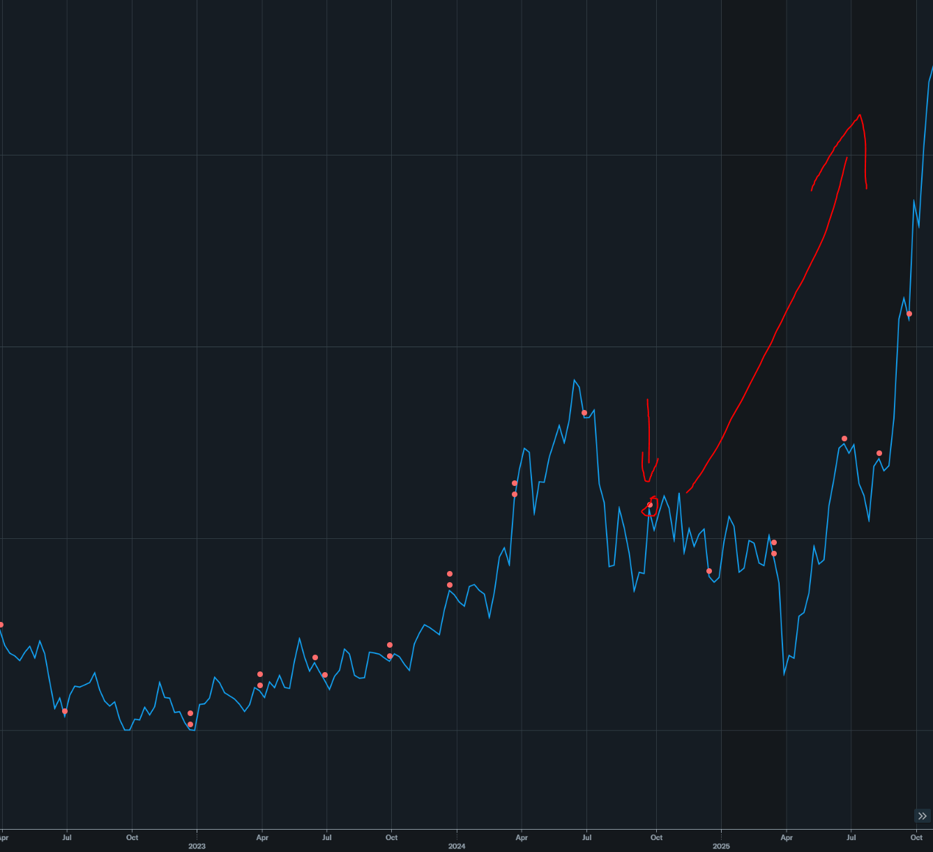
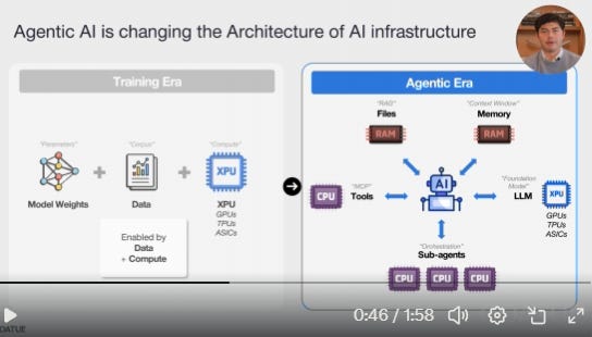
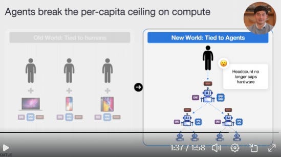
What finally got me to change my negative view on DRAM is a very nice video by Nick/Coatue.
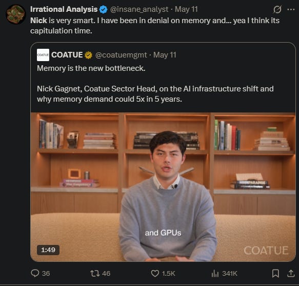

It’s a two minute video go watch it.
The thing is, someone told me a very similar thesis back at MS TMT when Micron was at $400/share.
Agentic AI adds huge structural demand.
Memory moon.
DRAM companies re-rate from price/book to price/earnings valuation.
At the time, I thought this person was a raving lunatic. Obviously very wrong…. but the question is…
Too late or more juice to squeeze?
If you go by the historical DRAM cycle length, we should be near peak cycle but because of AI agent demand (not a pull-forward of human demand) it is reasonable to assume the top is at least 18 months away from the time of writing (May 2026).
If you believe in agentic AI being a real, permanent demand driver, does mid-single digit P/E make sense for DRAM vendors? These guys are making so much money the forward book value is not terrible lol.
Sure there will be an overbuild and a cycle just like always. But this will be the longest cycle ever, with the most entertaining drawdown. But that is a problem for 18-months-from-now me to figure out.
A few people pinged me on May 11th that Coatue are idiots who top tick sectors like SaaS.
Congrats guys you were right. They did top tick memory but not in the way you were implying.
[4] Pitch: Samsung
So which of the three to choose? My views are closely aligned with Mustached Dr. Lisa Su, AKA TBU.
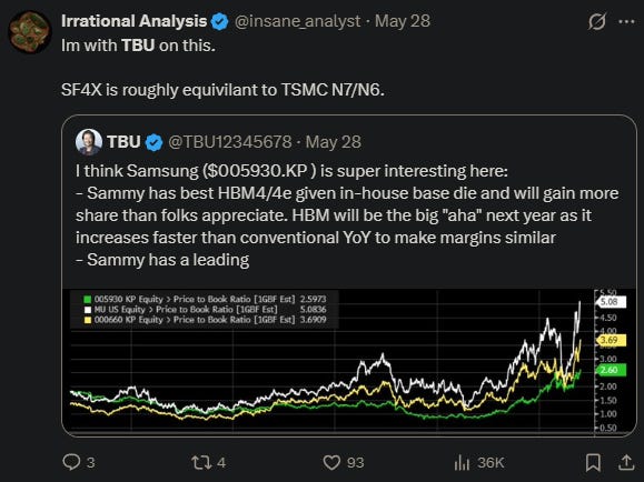
Samsung is the only DRAM maker with an in-house logic foundry and (more importantly) experience with interface IP and logic development.
I am very familiar with SF4X. At PPA level, it is competitive with TSMC N7/N6. Area is the biggest problem with that node. PFETs are also super leaky for some reason.
For first generation HBM4, SK Hynix chose TSMC N12 (wrong… why did you not pick N7…?) and Micron idiotically went internal DRAM process base die.
Going forward, SK Hynix and Micron will both have margins suffer from TSMC N3 base die and more importantly, neither has experience with logic design or high-speed signal integrity.
Samsung Device Solutions (logic foundry + DRAM + logic design) has lots of experience. Samsung in-house NVMe controllers are quite good.
What’s even better is Samsung Device Solutions has an internal silicon photonics process node and SiPho CPO design group. They had some decent papers at OFC recently. Not joking, I think Samsung Foundry SIPho is ahead of GloFo and S.LSI CPO group is ahead of AMD CPO group. This is partially a compliment towards Samsung DS, partially and insult towards GloFo and AMD.
Co-design opportunities are abundant.
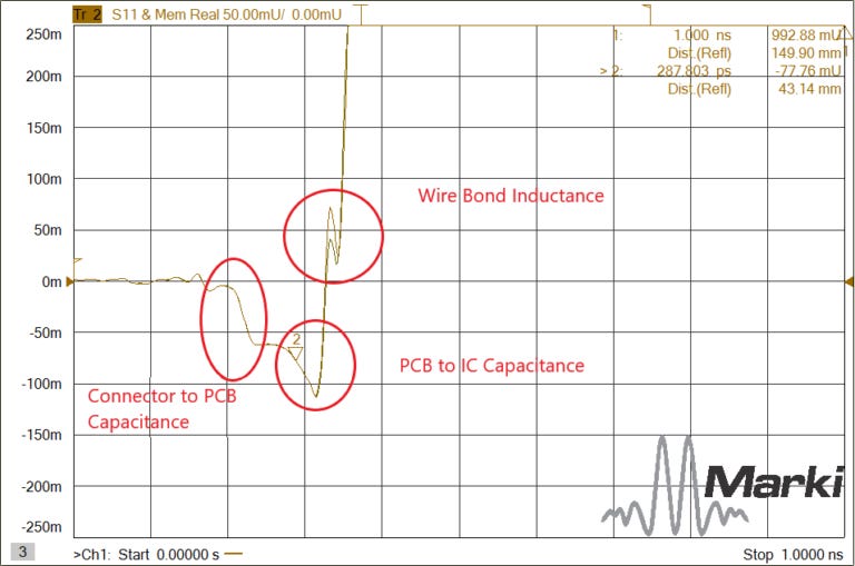
Rember the TDR traces I showed you earlier?
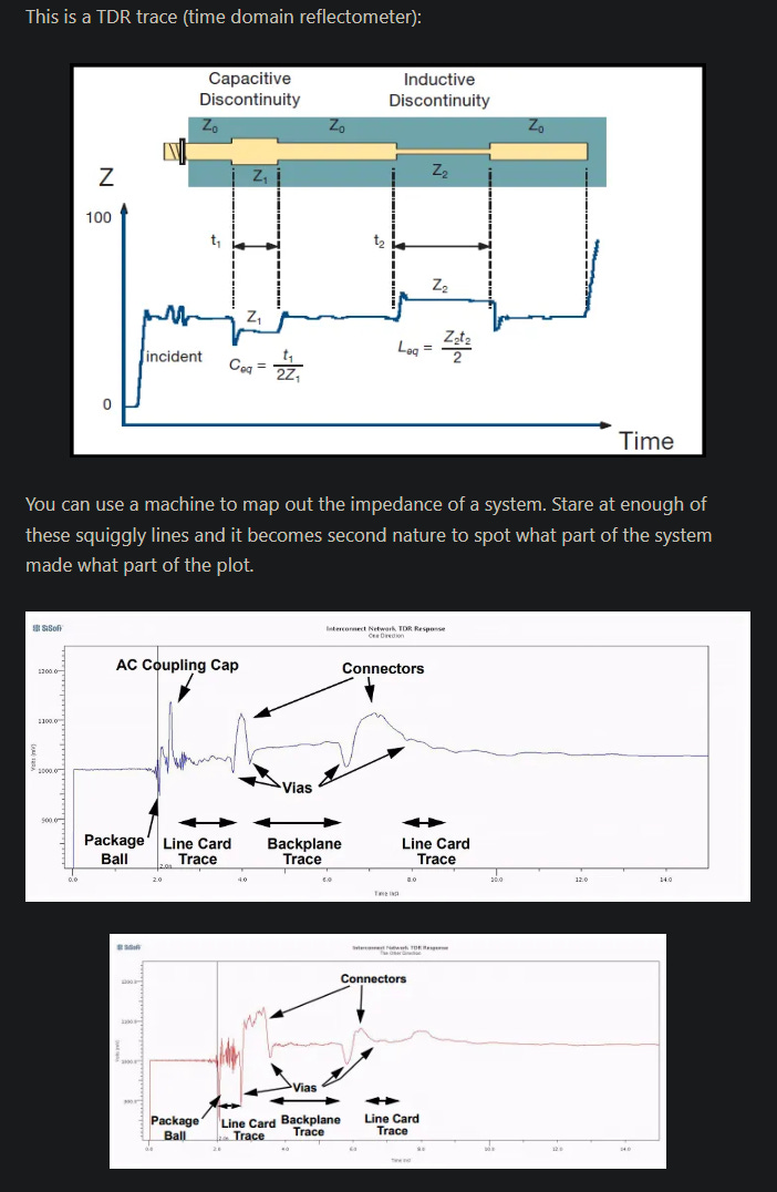
The frequency domain representation of the same thing is called s-parameters. Covered this in more detail previously many times go read backlog.
At a previous Hot Chips conference, Furiosia AI showed the s-param plots of their package design. (thank you Furiosia people, nobody else publishes these things publicly… very annoying)
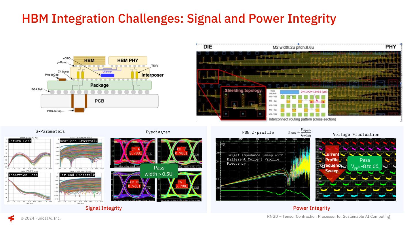
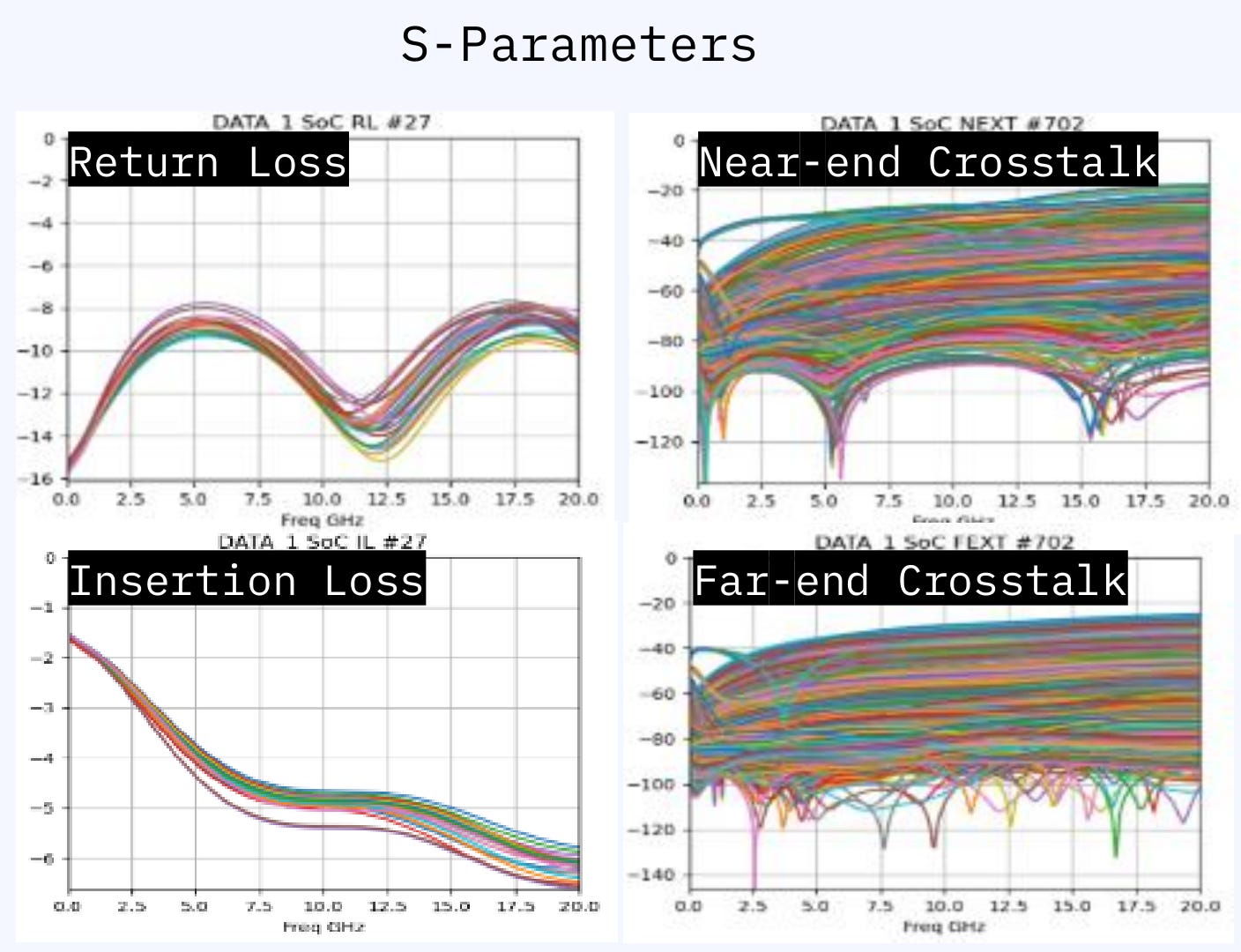
These are s-param plots for the package. (channel between ASIC and HBM base die)
There is another channel between the base die and the DRAM dies above. Those s-parameter plots are secret. I know roughly what they look like from experience but the exact magnitude of the impedance mis-match due to each layers bump capacitance and overall uniformity of the parasitic across each layer of a HBM stack is unknown to the public.
Samsung Electronics is in a unique position to aggressively co-design HBM PHY and TSV PHY to optimize DRAM design, HBM stack/process design, and interface IP design across electrical and optical.
If you know the channel ahead of time and can accurately model process variation of the channel, the SerDes can be aggressively optimized for that particular channel. THIS IS WHY NVIDIA NVLINK IS AHEAD OF EVERYONE. THEY DONT NEED TO INTEROPT. THEY CONTROL PACKAGE, PCB, SERDES, CABLES, EVERYTHING IN ENTIRE BIANCA/KYBER/WHATEVER PLATFORMS. NVLINK IS ETHERNET WITHOUT THE GENERALIZATION OR INTEROPRABILITY.
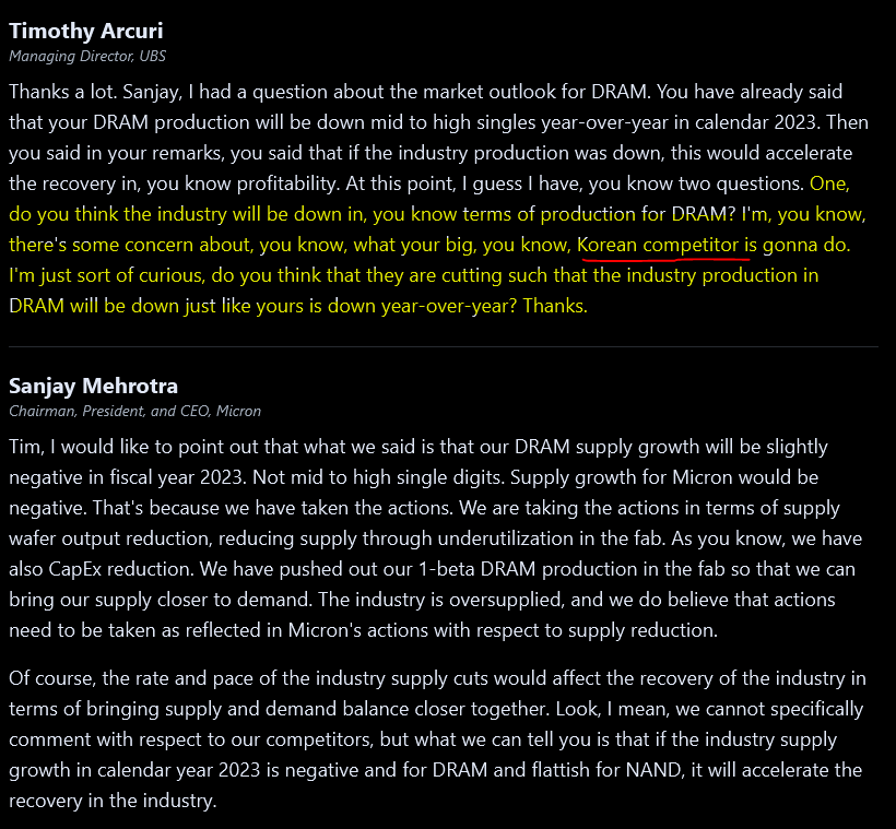
Now for stonks. I currently have no DRAM related position. Considering my options. Generally want to size it as $100K entry with option to double down and put another $100K. Only have direct access to Korean equities in un-levered long-only IBKR account so my personal list of options are:
Re-balance holdings, send $100K to IBKR account, buy Samsung equity.
Put $100K into KORU degen 3x levered Korea ETF in trading account.
$50K of micron calls (6+ month expiration) but the options chain looks like ass so unlikely.
Still debating this. Also to the uh…. 20+ finance people who have pinged me about memory over the last few months, please let me know what you think about Samsung » SK Hynix and Micron thesis. It’s more efficient to ping all of you simultaneously lol.
Seems like no-brainer to me. Cheaper on book value. Multiple structural engineering advantages.
This guy is slowly becoming washed up. None of this article actually covers what is the purpose of HBM in agentic AI systems? What is the pJ/bit for non HBM DRAM is. How much BW does different LLM models need dense vs MoE and plot this across active parameters. If he starts doing analysis from first principles, he might realize why there may still be upside for memory and storage stocks from here. He also seems to have stopped posting his account update this time, coz optical stocks are getting whacked and this guy is all in into optics. This guy is going to get cooked with that portfolio in the next 12 months coz optical isn’t 2027 story.
You set the trap in the history section and then walked into it on purpose, which is the fun part. "This time is different" is the phrase you flag at every Micron peak, and the agentic re-rating thesis is that same line in a better suit. Telling them apart comes down to being precise about where the cyclicality actually lives.
It was never really a demand story. Every prior cycle had real, growing demand too. the cycles came from supply racing to meet it and overshooting, and your own roast names the culprit each time: Samsung doesn't cut. So "agentic demand is permanent" can be entirely true and still not break the cycle, because what breaks the cycle is supply discipline, and that's the variable that has never held.
Which makes the price/book to price/earnings re-rating less a bet on demand durability than a bet on supply discipline finally sticking. The bull case quietly swaps "is the demand real" for "will the three of them stop knifing each other this time," and the section you just wrote is a long answer to that second question. Structural demand on top of undisciplined supply is just a longer cycle with a bigger top, which is close to where you land anyway. The re-rating needs the supply side to behave, and that's the one actor your own archive keeps convicting.