
[unfinished draft] It's the dataflow, stupid.
Groq is bigger than Mellanox.

Irrational Analysis is heavily invested in the semiconductor industry.
Positions will change over time and are regularly updated.
Opinions are authors own and do not represent past, present, and/or future employers.
All content published on this newsletter is based on public information and independent research conducted since 2011.
This newsletter is not financial advice and readers should always do their own research before investing in any security.
Feel free to contact me via email at: irrational_analysis@proton.me
Around two months ago, Nvidia acquihired Groq, taking all the valuable IP in a “non-exclusive” licensing agreement and (more importantly), hiring all the talent.
I am a long-time Groq hater.
Truly Irrational: Nvidia/Groq Deal

Irrational Analysis is heavily invested in the semiconductor industry.
Here is an old post from February 2024 that was specifically written to shit on Groq.
![[V]ery [L]ong [I]ncoherent [W]riteup](https://substackcdn.com/image/fetch/$s_!lVhT!,w_1300,h_650,c_fill,f_webp,q_auto:good,fl_progressive:steep,g_auto/https%3A%2F%2Fsubstack-post-media.s3.amazonaws.com%2Fpublic%2Fimages%2F1335e244-45bb-4add-a677-d9ab1ed74702_875x957.png)
My immediate reaction was this deal was a bribe to get H200 exports approved by the Trump administration. Many others have publicly expressed this view and privately messaged me as well.


Even many of Nvidia’s own employes thought this was a bribe.
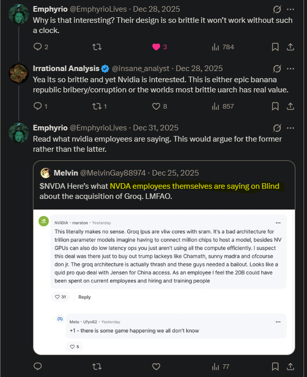
Note: Blind is a (particularly cancerous) social media platform that requires you to sign up with your work email. They don’t check if you still work at the company you signed up with though.
But after spending months thinking about this, and in light of recent developments in AI economics, I have fully capitulated.

It started with a simple (non-engineering) premise.


Groq raised LITERALLY LESS THAN THREE MONTHS BEFORE NVIDIA DEAL at a $7B valuation. Don Jr VC firm (1789 Capital) was in the round.
A $14B buyout would lead to 100% return on investment for Don Jr. in less than three months. Feels like an appropriate sizing to theoretical bribe.
But $20B deal effectively invalidates the bribery theory. It’s way too high.
$20B is the kind of money that says “shut the fuck up, stop negotiating, and get your ass into Nvidia offices by next week”.
Which is what happened.

It took only four business days to get Groq talent in the door and working from the time this deal was publicly leaked/announced. Clearly, there is an urgency at Nvidia, and there is even more evidence on this front…
My sense is OpenAI was bidding for Groq and Jensen beat them to it.
I guess Groq employees were more interested in real money rather than theoretical money. Being rich on paper but poor in real life must not be a great feeling all these years parading a Llama around like clowns.

Continuing this introduction, let me bring up an old post that was half about Tenstorrent, half about why I thought (at the time) vast majority of AI hardware startups would fucking die.
Tenstorrent and the State of AI Hardware Startups

Irrational Analysis is heavily invested in the semiconductor industry.
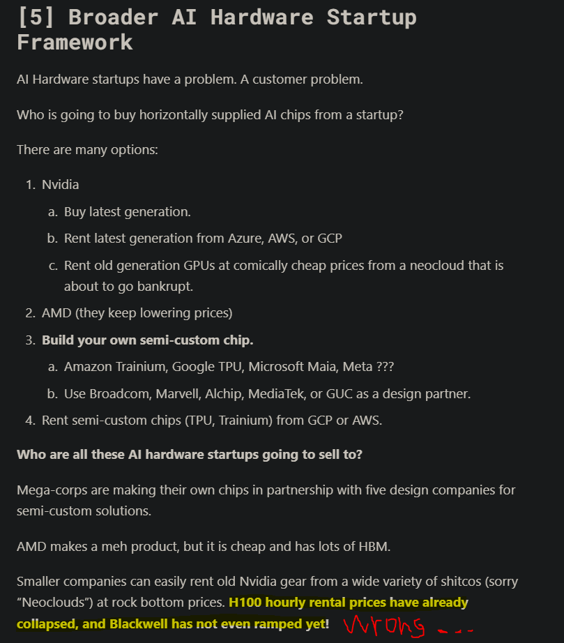
In this deep dive, I have four primary objectives:
Explain complete reversal on prior negative view of all AI hardware startups.
Explain complete reversal of prior hatred towards Groq architecture.
Cover all the interesting AI hardware startups. (Groq, Cerebras, D-matrix, SambaNova, Etched, Positron, MatX, Tenstorrent, Taalas)
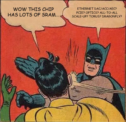
EXPLAIN WHY NONE OF THIS IS ABOUT SRAM.
https://en.wikipedia.org/wiki/It%27s_the_economy,_stupid
It’s the dataflow, stupid.
<todo better thumbnail>

THIS IS AN UNIFINISHED DRAFT
I am presently in negotiations with MatX, Etched, Taalas, and Positron for access to technical information and permission to publish content relevant to their sections.
The other AI hardware startups have enough public info to cover.
Given how important the Groq deal is to public markets, I have decided to publish an early (very incomplete) draft that only has Groq and excludes all the startups.

Unironically, I believe Groq deal is bigger than Mellanox.
Full reversal/capitulation here. For years I have attacked Groq. There are reasons for prior view and new view… which hopefully are explained somewhat coherently in section [5+6].
There are a variety of notes (to myself) in <> throughout as I plan to duplicate this post and fill in the missing sections later. Not happy with this quality of work but had to make this compromise.
AI hardware startups get to see private drafts of their individual sections, debate facts, and veto information they wish to stay confidential. But no opinion altering. There is going to be some back and forth that will take months potentially. Really want to include proper technical coverage of all four under-negotiation startups.
<todo: rewrite this section for final post>
<todo: update disclosures with extra shit for final post>
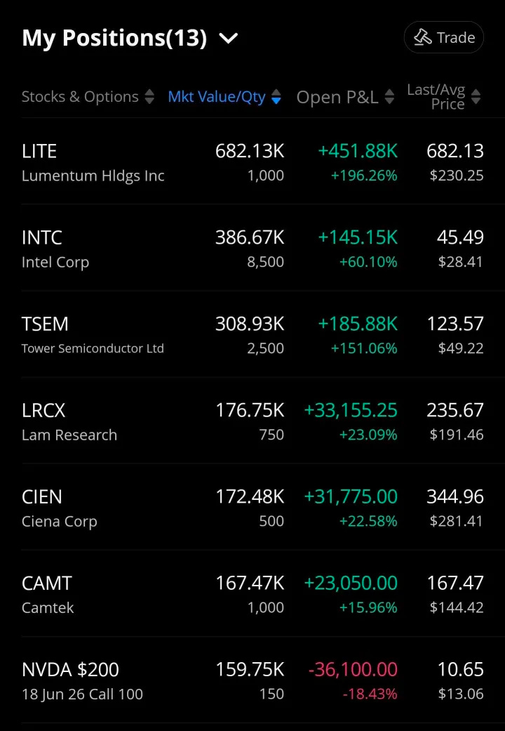
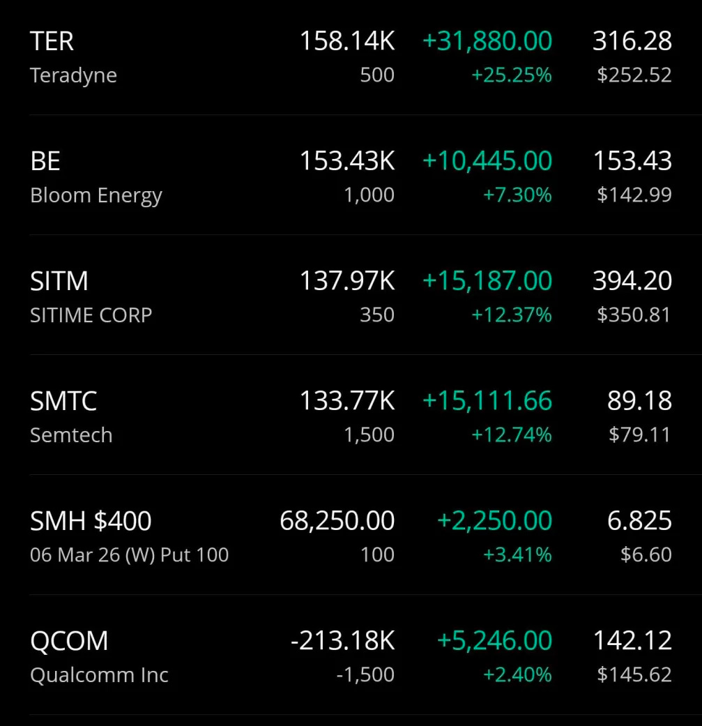
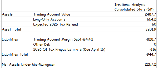
At the time of writing I have the following state in my trading account.


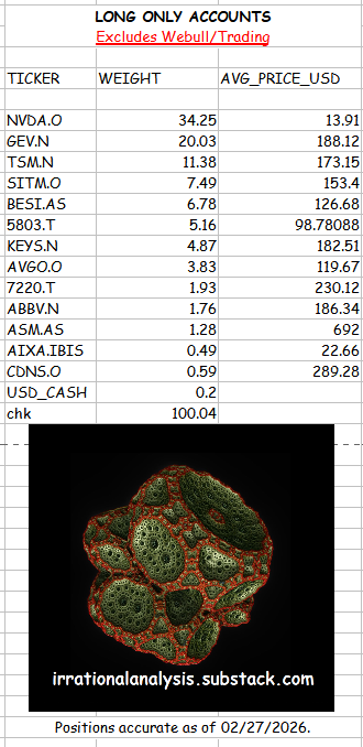
And here are the long only-accounts with some consolidated stats.
You can assume I am biased because I own a huge amount of Nvidia shares and call options. But in truth, I have these positions for orthogonal reasons.

You know my biases, go make up your own mind.
Maybe I know more about semiconductors than you?
Contents:
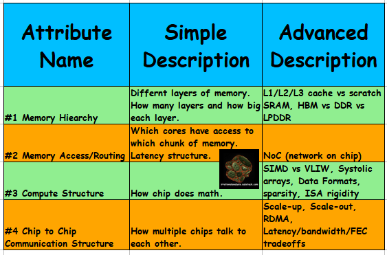
How to describe any computer.
Memory Hierarchy
Memory Access/Routing
Compute Structure
Chip to Chip Communication Structure
Normal Architectures
CPU (AMD Genoa-X)
CPU (Intel Saphire Rapids)
GPU (Nvidia GB300 // Blackwell Ultra)
TPU (Ironwood // V7)
Tenstorrent <todo>
Positron <todo>
Abnormal Architectures <todo>
D-Matrix <todo>
Cerebras <todo>
SambaNova <todo>
Etched <todo>
MatX <todo>
Taalas: Very Abnormal <todo>
Groq: Batshit Insane and Unhinged
Nvidia Incredible IP Synergies with Groq-Style Architecture
Clock-Forwarded SerDes
Hybrid Bonding
Leading Thermal Team
Theoretical Optical Global Clock
Mock-Up of Possible Nvidia/Groq Product
Any Idiot Can Build a Bridge // Golden-Age for Unhinged Computers
[1] How to describe any computer.
Today’s material is going to be complicated, so we need a generalized framework.
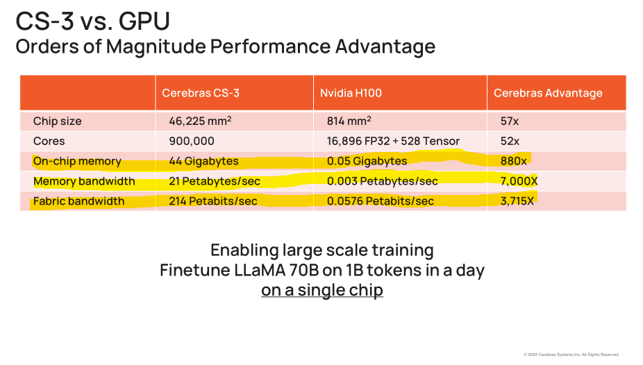
For example, Cerebras loves to make bullshit claims against Nvidia, neglecting to mention the nuance that the individual cores are very small and thus the compiler needs to perfectly map neural network graphs onto a giant mesh before runtime.
This is a great example of how “memory access/routing” is a key attribute of a computer.
I believe that any computer can be reasonably described in such a way that high-level comparisons of vastly different architectures is possible using only four attributes.
I have a previous guide on computer architecture but want to sort of re-write it just for this post. Very strange architectures require coverage in a new way.

[1.a] Memory Hierarchy
The classical way to describe this concept is with a pyramid.
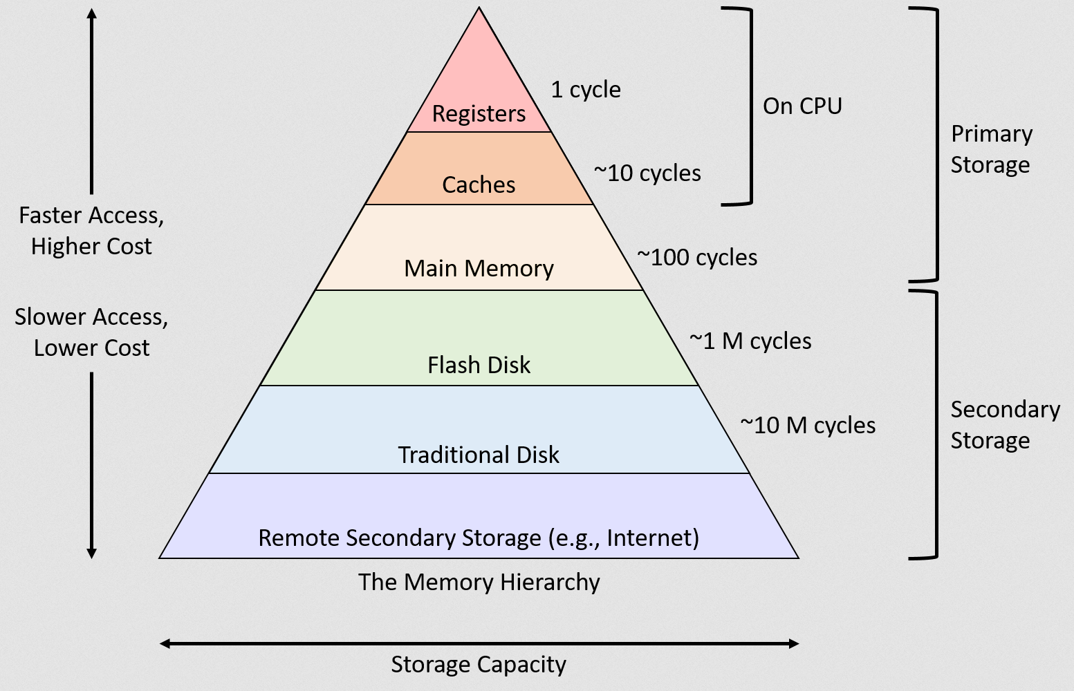
Going up the pyramid leads to exponentially better performance and higher (worse) cost.
In the old days, most computers (various CPUs basically) would have 3 levels of cache.


Cache is (almost always) made of SRAM but is not the same as SRAM.
During runtime, a compute core needs to decide what memory should go where. For example, should a particular variable be stored in L1 for super fast access, or kicked to L3 for fast access, or kicked all the way to DRAM because it’s not important?
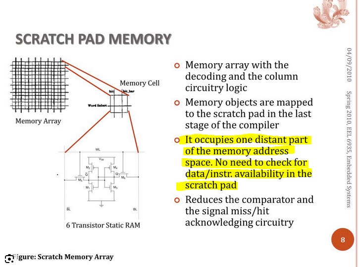
If the hardware is making these decisions, the SRAM (on-chip memory) is a cache.
If software makes these decisions, the SRAM (still on-chip memory) is a “scratchpad”, NOT A CACHE.
, 캐시(Cache) 메모리 비교 : 네이버 블로그")
This is a very important nuance that most public discourse completely fucks up. Frankly infuriating. Completely changes very fundamental aspects of the system, from memory address maps to compute hardware complexity to programming model.

Key questions you should ask when evaluating a computer architecture using principal #1 (memory hierarchy):
Does the system use a cache or a scratchpad.
What is the penalty for cache misses?
Are there multiple levels of cache or scratchpads?
What is the ratio of cache/scratchpad to DRAM or other layers of memory?
[1.b] Memory Access/Routing
Now let’s go up one level in the stack.
Given an arbitrary chunk of memory, how does an arbitrary chunk of compute access said memory?
Yes, data typically moves from an HBM stack to the logic die. Gold star for you. But how does the data move within the logic die?
The key concept is NoC, network on chip. Dr. Ian Cutress has a great video on this. Best on the internet.
Two primary architectures are used to connect elements on a chip.
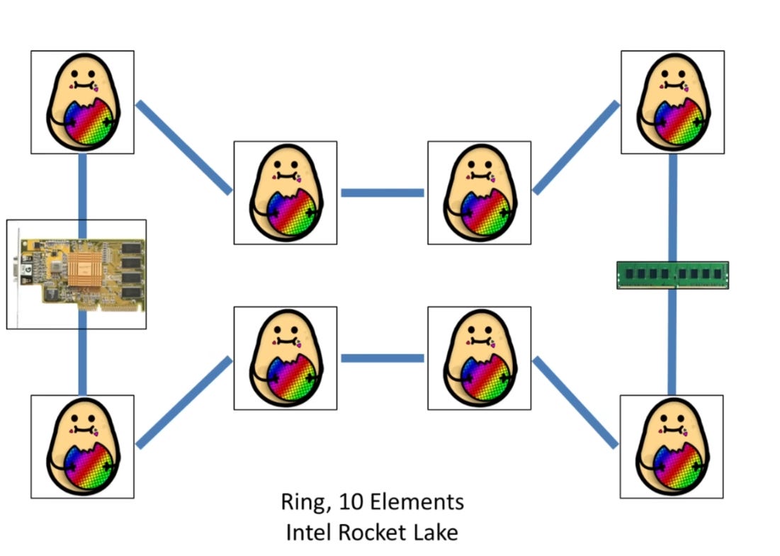
The first is a ring,or set of rings.
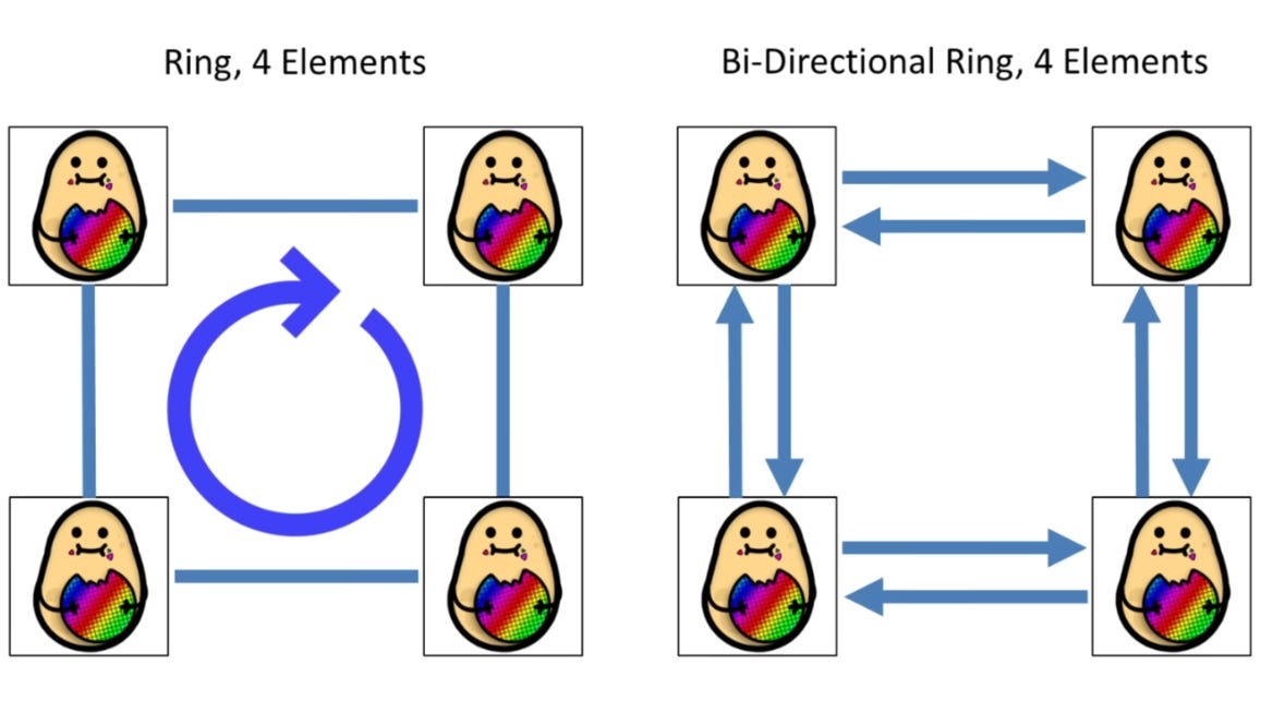
The second main type is called a mesh.
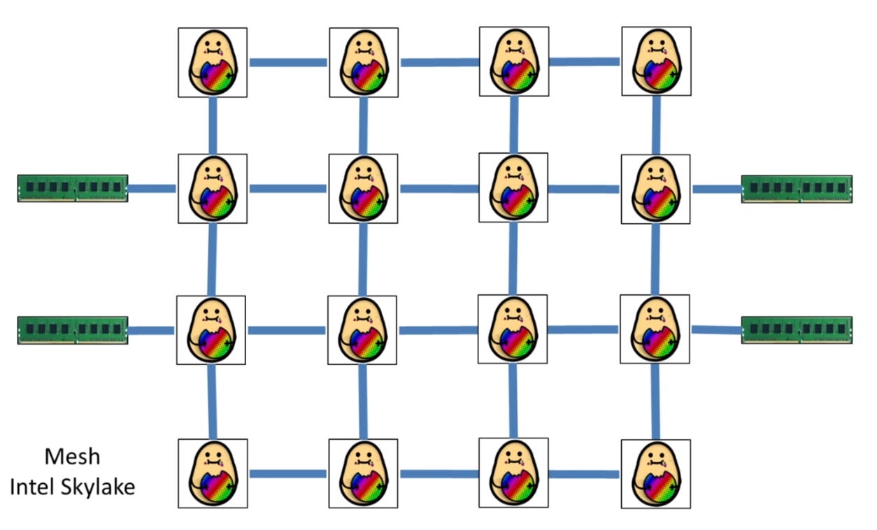
And derivatives of a mesh.
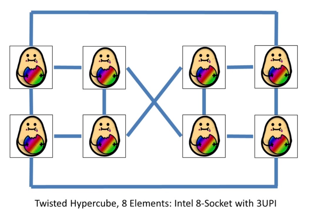
There are many more fun combinations that I will skip in the interest of time. Many of these are proprietary and I probably shouldn’t write about them here.
You can have multiple ring buses where some elements are only on a particular ring.
Can also have a crossbar that groups a cluster of elements which then connect to the wider chip via a ring or mesh.
Not all elements on the chip need to have a path to every other element.

Remember, memory (block of SRAM, HBM stack) is just a node on the NoC.
HOW THE NETWORK ON CHIP IS SET UP MATTERS A LOT.
[1.c] Compute Structure
This resource is a hidden gem.
https://www.lighterra.com/papers/modernmicroprocessors/
In the interest of time, I will go very fast and handwave a lot. It is probably easier to learn from examples in latter sections anyway.
Computers perform math in basic units called instructions.
Example instructions:
load a byte from memory to a register
addition
logical and/or/xor
….
Now the key questions are:
How “fancy” is your computer?
How many data operands does the computer use at once?
What data formats are supported?
[1] Fancy compute cores use cool strategies such as branch prediction, speculative execution, and out-of-order execution. These strategies all “break” the original complied code in some way. The hardware itself figures out shortcuts in the assembly code in real-time. Fancy computers (CPUs basically) give great performance boosts at the cost of area/power and parallelism/scalability. This is the main reason CPUs suck for AI.
[2] The fundamental differentiator between a GPU and a CPU is the idea of warps/waves.


Single-instruction, multiple data (SIMD) is the architectural principal by which GPUs work. Nvidia uses 32-element “warps”, while AMD uses 64-element “waves” in datacenter. All AMD architectures were wave64 but a few years ago they moved gaming architecture to wave32.

Over the years, CPUs have added SIMD instructions. A lot of SIMD instructions…
https://en.wikipedia.org/wiki/List_of_x86_SIMD_instructions
https://en.wikipedia.org/wiki/AArch64#Scalable_Vector_Extension_(SVE)
GPUs dominate AI workloads because they are (this is oversimplified…) mostly pure SIMD machines while CPUs have SIMD stapled on.
Many of the exotic architectures to be covered in this post are SIMD machines but much less flexible than a GPU.
Let’s talk about data formats and sparsity.
In the old days, only single-precision (32-bit) and double-precision (64-bit) floats mattered.
With AI, floats and int down to 4-bits matter.
For example, Cerebras idiotically does not support 8-bit floats. STILL THEY DO NOT SUPPORT THIS BASIC FEATURE. Nvidia already has 4-bit floats and AMD will support FP4 soon.
They also make bold claims about unstructured sparsity. I have asked ML people for years about this and to this day none of them have found a use for this feature.
With lower precision data formats, you lose some accuracy but gain much more throughput.

With some work, the accuracy penalty can become negligible.
Finally, let’s briefly cover very-long-instruction-word (VLIW).
Deep dive here:
Short answer (oversimplified) is…
VLIW = SIMD but the instructions can be all different but with many constraints.
A “bundle” of instructions (say… 1 load, 5 mult, 2 add, 1 store, 2 branch) is operated on in a block. The compiler must schedule each bundle/block.
Very simplified hardware design, satanic nightmare compiler burden.

[1.d] Chip to Chip Communication Structure
The simplest chip-to-chip (c2c) communication structure is all-to-all.


Nvidia uses a full all-to-all over passive copper which is the best in terms of performance and flexibility but the worst in terms of cost and reliability. Ask around about the legendary cabled backplane. :)
Each GPU can talk to any other GPU in the NVL72 domain via a single hop, at full bandwidth.
Google uses a 3D-Torus for their Ironwood TPU.
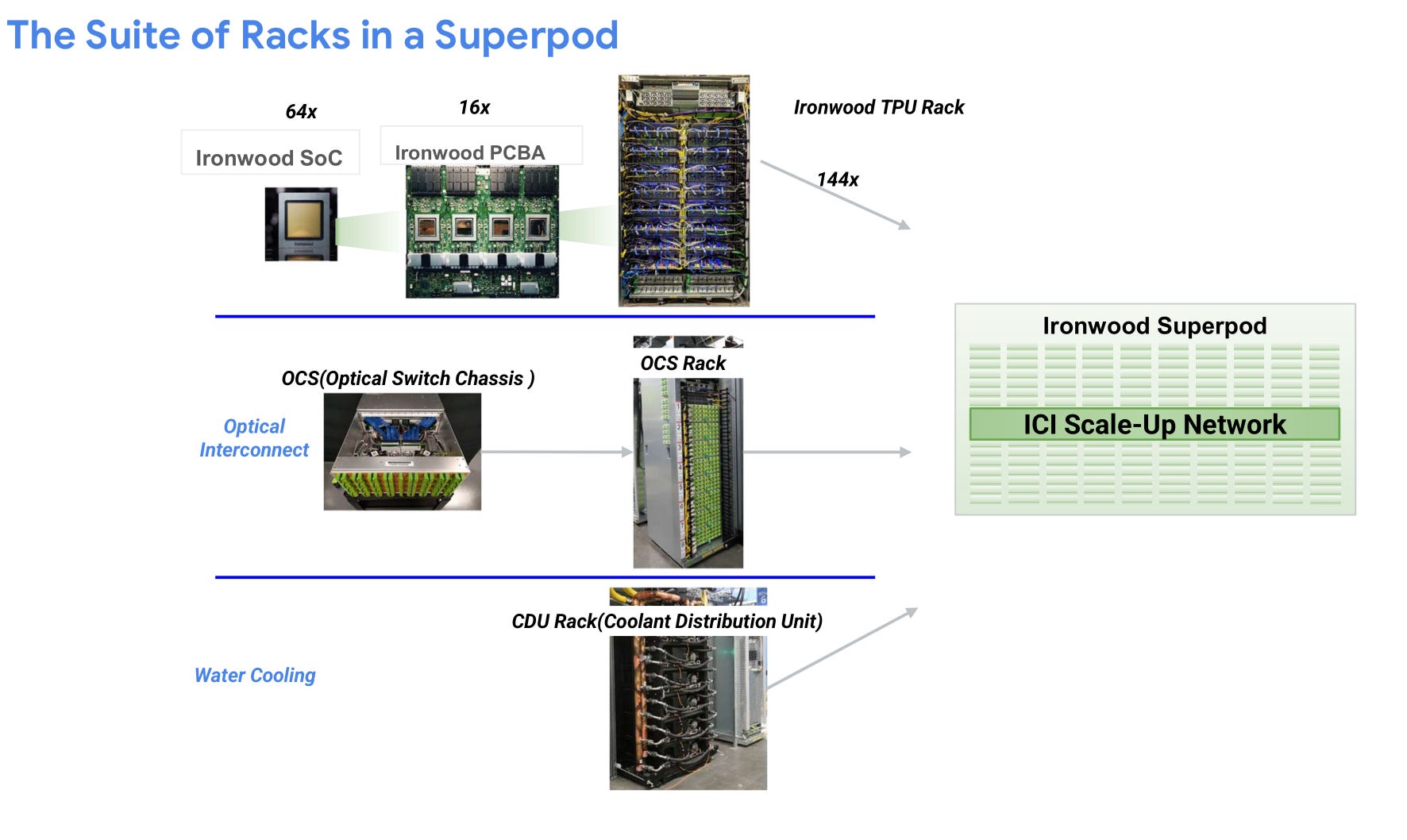
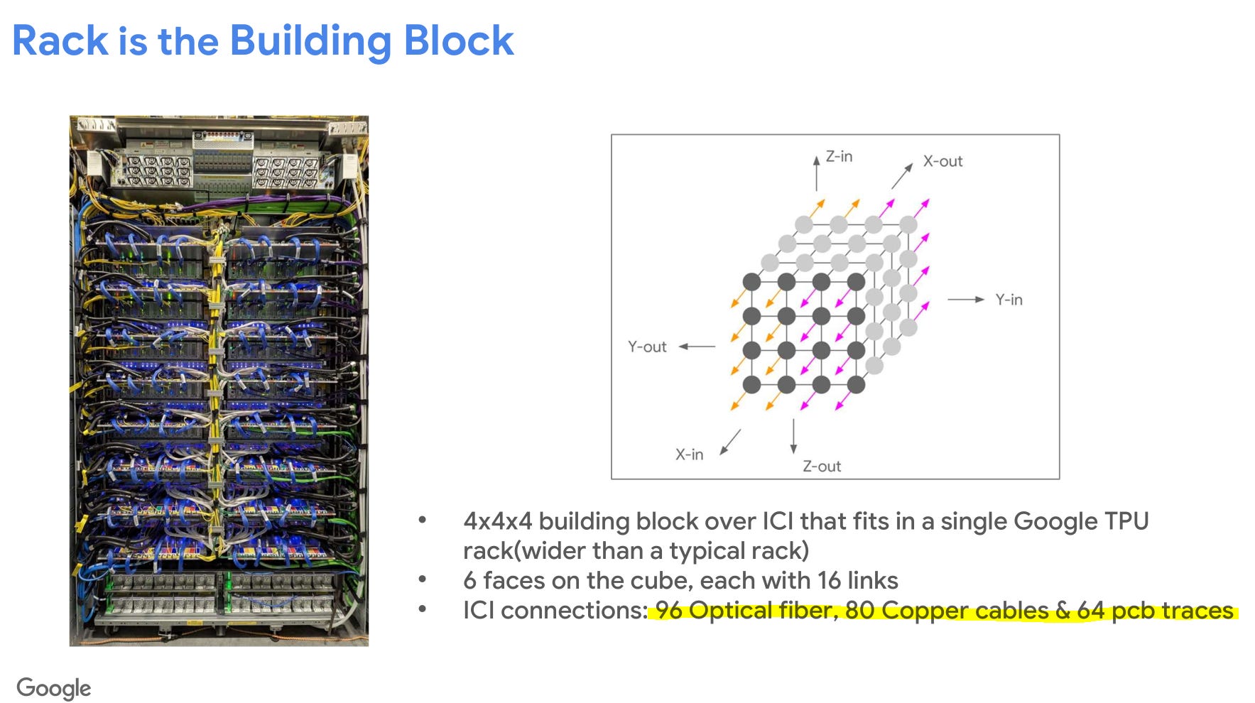
Each block of 4x4x4 (64) TPU chips are connected electrically within a rack. The cross-rack connections are optical via mems-based OCS.
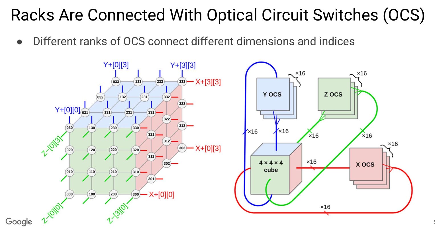
This is much more reliable and cost effective than Nvidia’s strategy but makes the compiler far less flexible. Programmers need to account for the non-uniformity of the network, both in terms of latency and bandwidth asymmetry.
Finally, there is the dragonfly topology future TPUs will use. The real TPUs made by Broadcom.
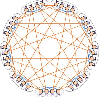
https://research.google.com/pubs/archive/34926.pdf

Mr. Abts is going to show up again several times.
[2] Normal Architectures
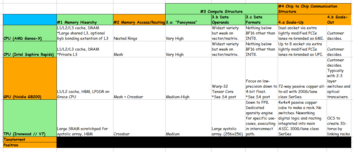
Summary table here for the lazy.
<todo update table>
[2.a] CPU (AMD Genoa-X)


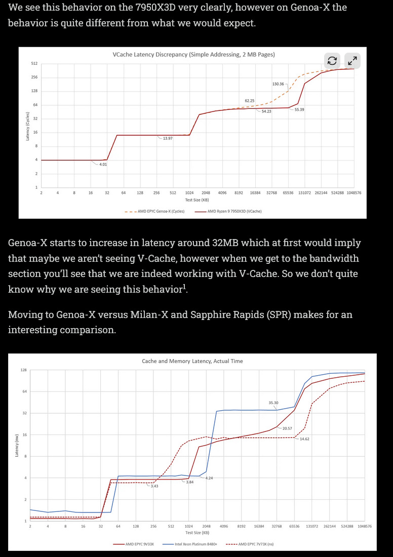
AMD utilizes a nested ring architecture for their NoC. Each CCD (CPU core chiplet) is a ring that connects to the I/O die. All the memory interfaces also connect to the I/O die.
Special SKUs (-X series) have extra SRAM dies hybrid bonded onto the CCD dice.


This strategy slaps a huge cache SRAM extinction for L3. Due to the physical locality, L3 latency is modestly effected.

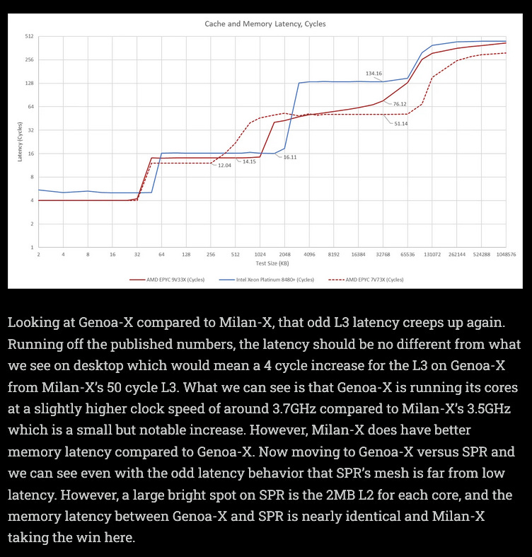
The key points I want to make sure nobody misses are as follows:
AMD -X SKUs extend cache SRAM. SPecifically L3 cache.
Even though AMD publicly claims there is no latency impact, independent testing by Chips and Cheese show some minor/strange performance penalties.
Stacking SRAM on top of compute is very difficult. AMD chose to avoid this problem by only stacking the SRAM die on top of existing SRAM. Notice the two “structural” (spacer) dies over the CPU cores themselves.
Design choices made by AMD are instructive for understanding Groq and D-Matrix roadmaps.


[2.b] CPU (Intel Saphire Rapids)

Intel Saphire Rapids has a more traditional mesh NoC. Remember, it takes multiple hops for DRAM data to make it to cores in the middle. Also note that certain on-die accelerators (mini ASIC) such as QAT and DSA are in their own block with a dedicated mesh node.
Cache (SRAM) is spread out via the purple blocks.

Note that AMD has a large 32 MB shared L3 cache per 8-core Genoa CCD while Intel choses to make L3 cache private per core in 1.875 MB/core chunks.
Key points:
Cache/SRAM design has many tradeoffs.
Bigger shared cache means more latency, but all compute cores can use the same memory.
Bigger blocks of SRAM are not always better.
Lot of nuance that depends on the core microarchitecture and NoC design.
[2.c] GPU (Nvidia GB300 // Blackwell Ultra)
. Callouts highlight PCIe Gen 6 (256 GB/s), NVLink v5 (1,800 GB/s to NVSwitch), NVLink-C2C (900 GB/s CPU–GPU), and 288 GB HBM3E (12-hi stacks, up to 8 TB/s).")
Notice the large shared L2 cache across two GPU clusters. The D2D is clock-forwarded.
 architecture showing CUDA cores, Tensor Cores, TMEM, shared memory, SFUs, Tex blocks, and other SM units.")
Warp scheduler is 32 thread per clock. This is the historical (SIMD) backbone of GPUs. The tensor cores can be interacted with in many ways. SA has great coverage so just go read that.

Nvidia uses a mesh NoC within the GPC while the gigathread engine is a crossbar. In other words, meshes attached to a crossbar.
[2.d] TPU (Ironwood // V7)
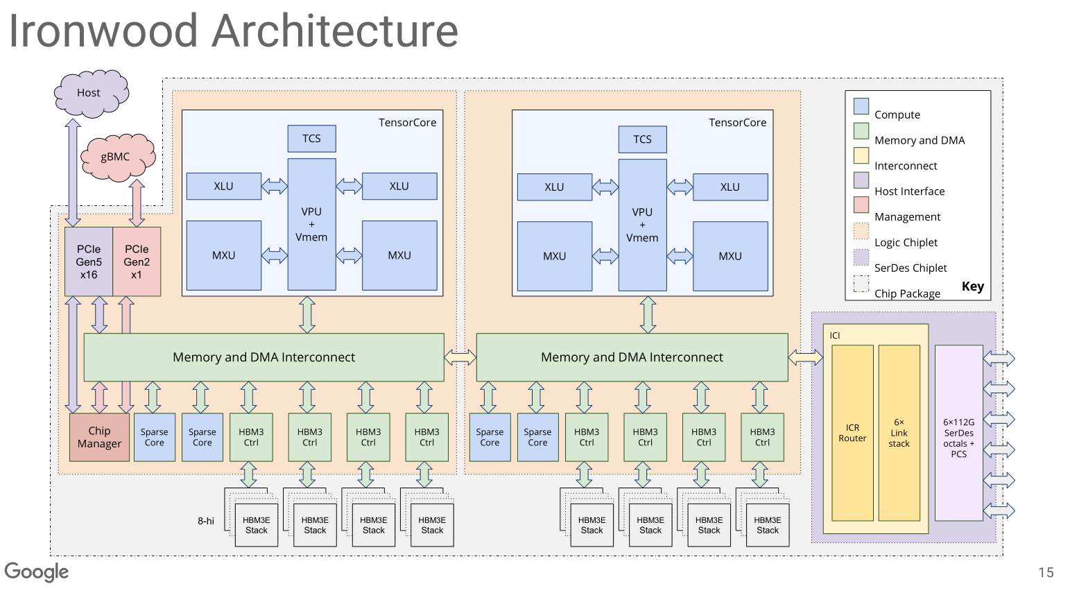
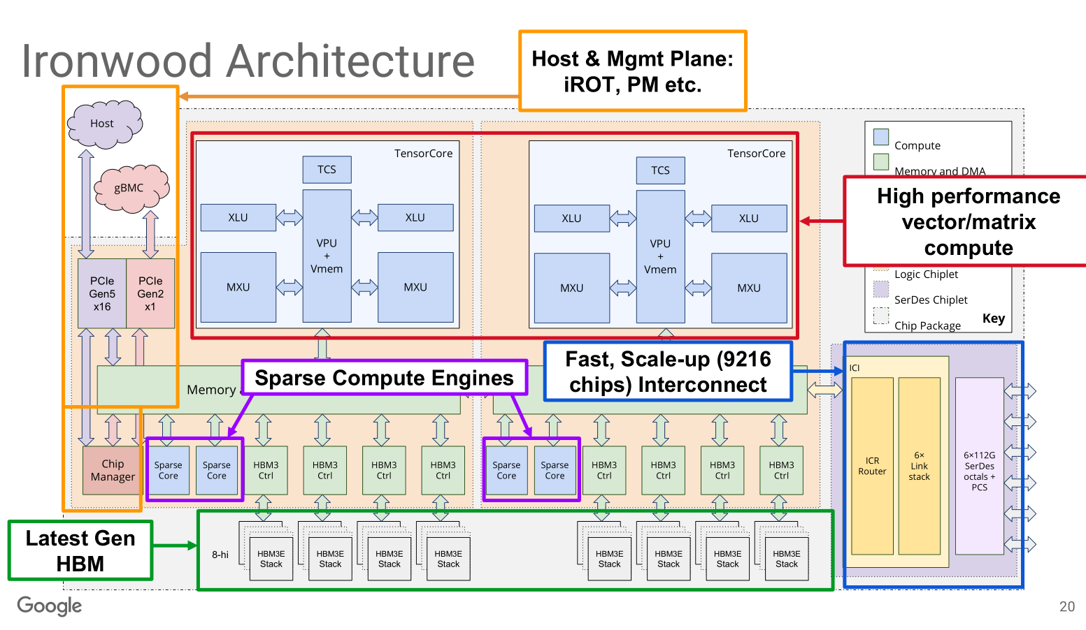
Google uses a crossbar NoC and has integrated routing (yellow box) on-chip. This means there are no switches equivalent to say a NVLink switch for scale-up.
The compute is built around a 256x256 systolic array as the main compute engine for matrix multiplies. Control is handled by an 8-wide VLIW core. You can think of the 8-wide VLIW as a controller.
A compiler must generate instruction bundles ahead of time.
![V]ery [L]ong [I]ncoherent [W]riteup](https://substackcdn.com/image/fetch/$s_!HXG5!,f_auto,q_auto:good,fl_progressive:steep/https%3A%2F%2Fsubstack-post-media.s3.amazonaws.com%2Fpublic%2Fimages%2Fd1f5299d-d323-425c-82b6-05a935d1f315_2970x1700.jpeg "V]ery [L]ong [I]ncoherent [W]riteup")
It is very important to understand that the SRAM on a TPU is not a cache.
It is a scratchpad used to feed a systolic array.
https://en.wikipedia.org/wiki/Systolic_array
Systolic arrays are dataflow compute structures.
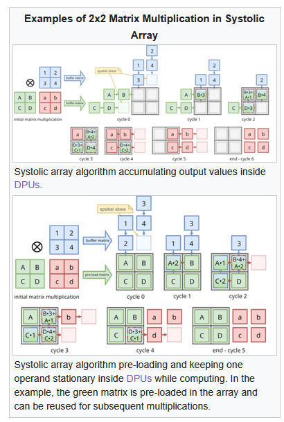

Most of the AI hardware startups use systolic arrays of varying sizes and configurations. Google themselves have changed the size of the systolic array across TPU generations. There is a lot of complexity in deciding the size and shape of a systolic array for accelerator design.
[2.e] Tenstorrent
<todo>
[2.f] Positron
<todo>
[3] Abnormal Architectures <todo>
<todo>
[3.a] D-Matrix <todo>
<todo>
[3.b] Cerebras <todo>
<todo>
[3.c] SambaNova <todo>
<todo>
[3.d] Etched <todo>
<todo>
[3.e] MatX <todo>
<todo>
[4] Taalas: Very Abnormal <todo>
<todo>
[5] Groq: Batshit Insane and Unhinged
Groq is very polarizing within industry for several key reasons.
Anyone who has a basic understanding of computer architecture immediately understands the abomination they have created.
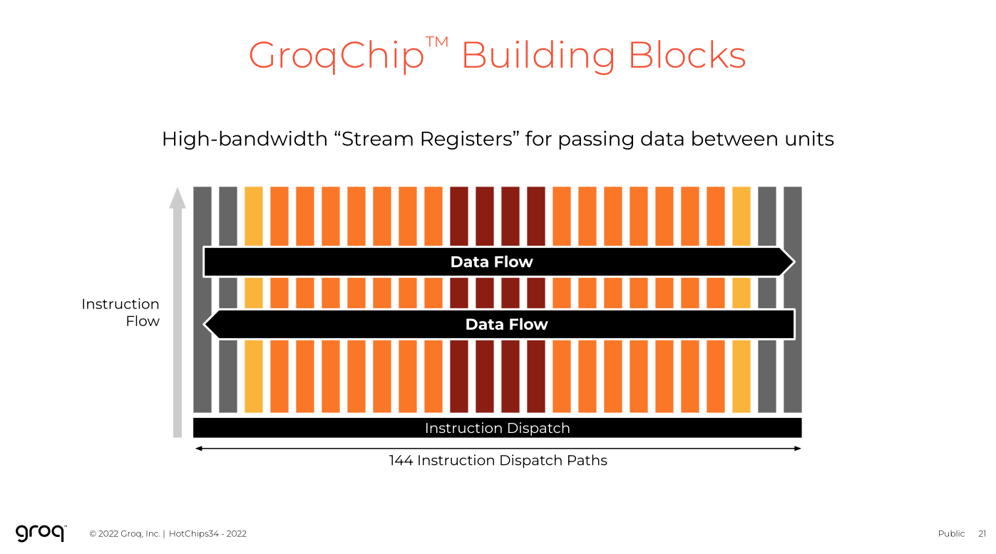
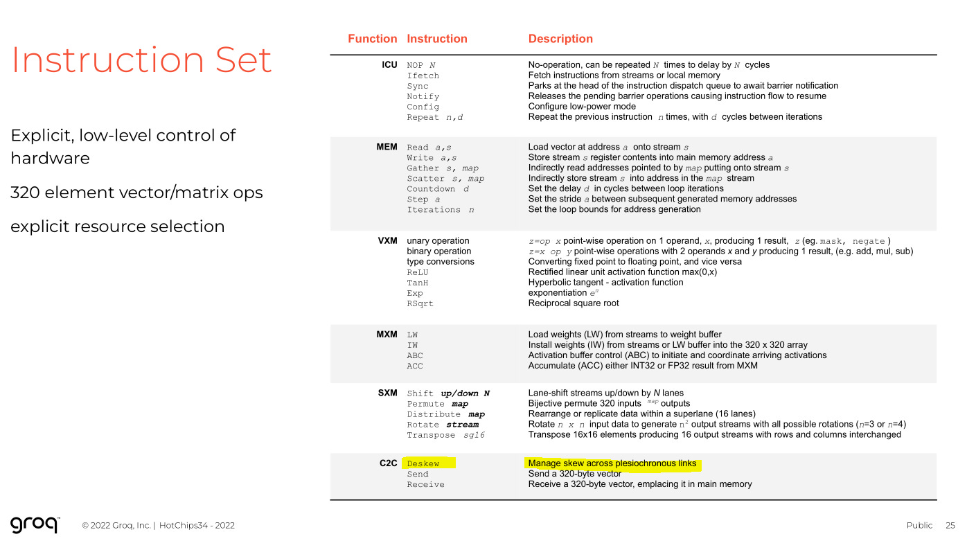
Proclaims all the magic benefits of 144-wide VLIW without addressing any of the downsides.
Built a retarded “cloud business” with ancient 6-year old chips build on trash GloFo 14nm process.
Lost money on every token generated within bullshit cloud buisness.
The largest VLIW bundle size people have tried is 8. These degenerates went 144-wide.
One particularly annoying investor.


I have had multiple verbal arguments with one fashionable Groq employee who repeatedly claimed that the architecture is not 144-wide VLIW.
“We created something different.”
BULLSHIT
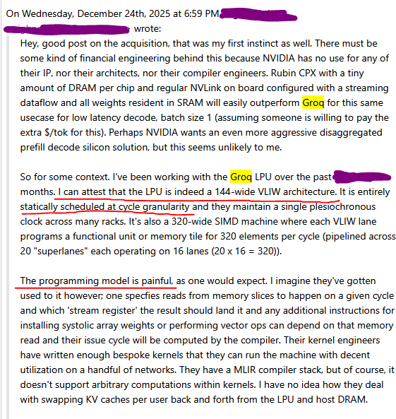
Engineers who have used Groq Cloud understand the chip is 144-wide VLIW that requires cycle-granularity static scheduling from the compiler.
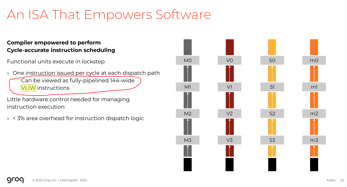
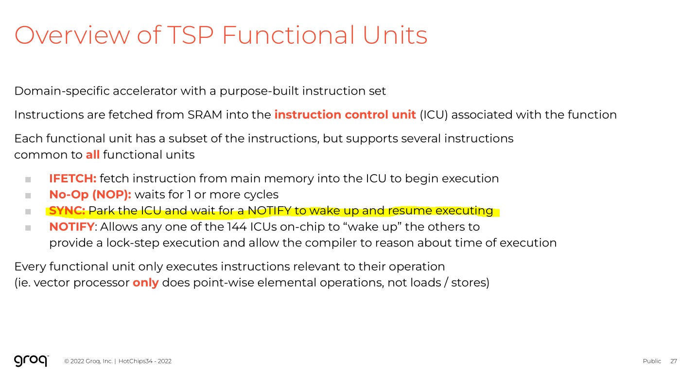
Groq’s own public presentation at Hot Chips 2022 EXPLICATLY ADMITTED THE ARCHITECTURE CAN BE VIEWD AS 144-WIDE VLIW.

Dennis Abts, the CHEIF ARCHITECT of Groq presented at Hot Chips, admitted to 144-wide VLIW, and then literally joined Nvidia one month later.
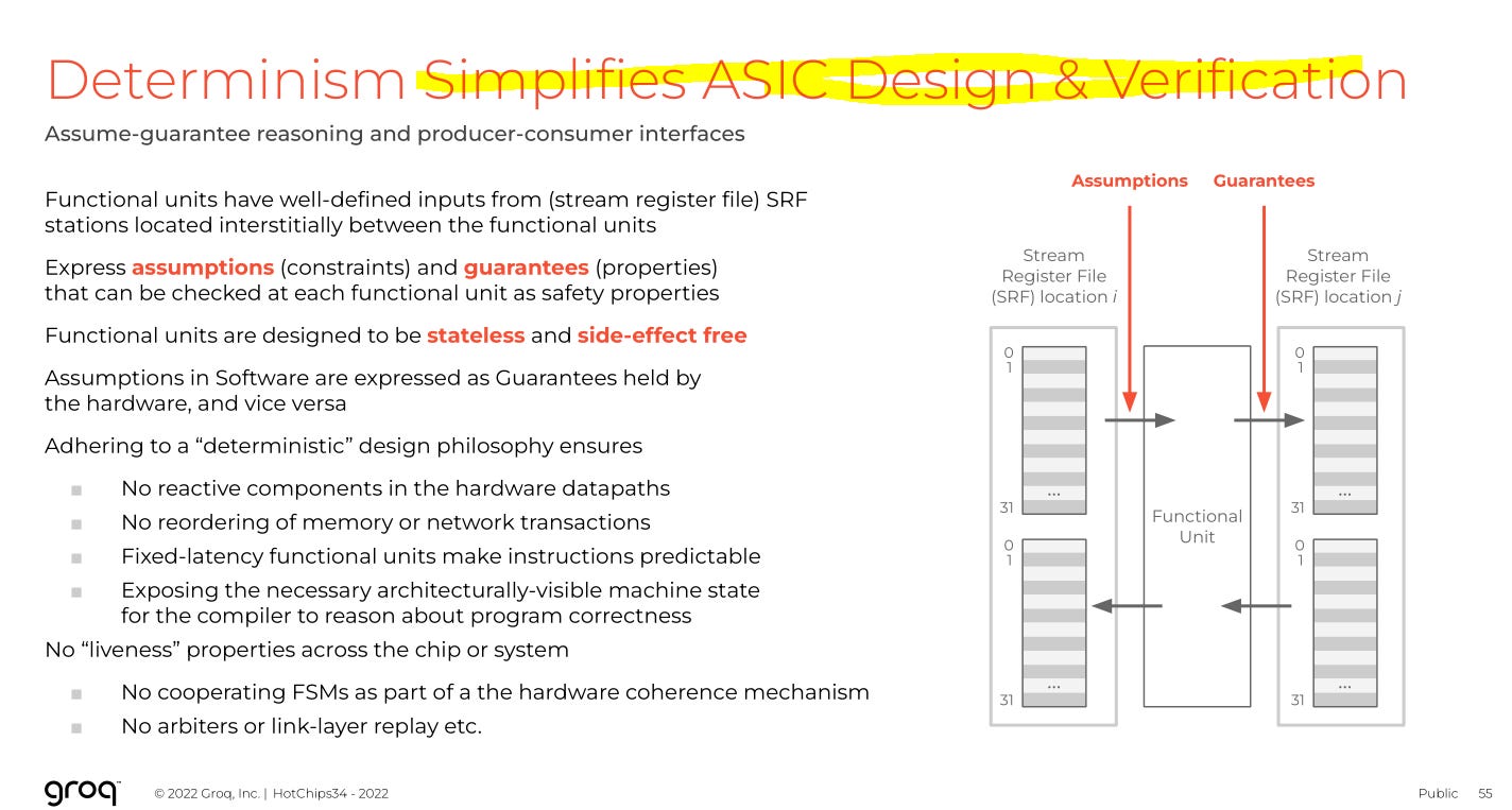
Groq is a dataflow architecture, but in the most unhinged, revolting, insane way possible.
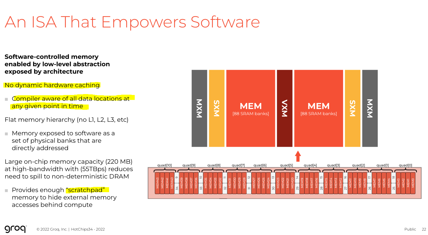
Scratchpad SRAM. Compiler has to cycle-accurate schedule everything ahead of time.
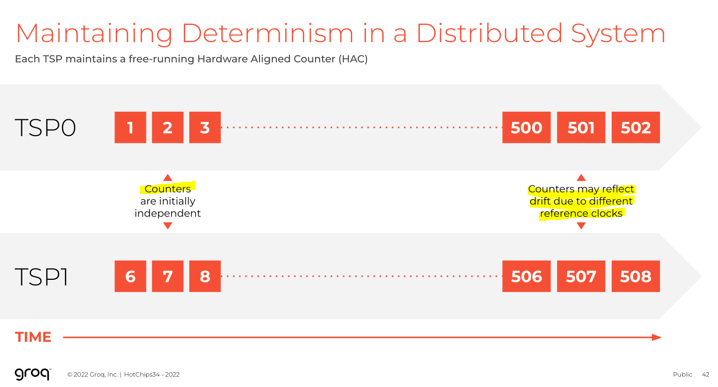
They have to synchronize all chips as best they can. EVERY CHIP IN EVERY SERVER ACROSS EVERY RACK.
This compiler bursts into flames the moment there is the slightest synchronization hiccup.
If synchronization is bad, they have to park all the compute.
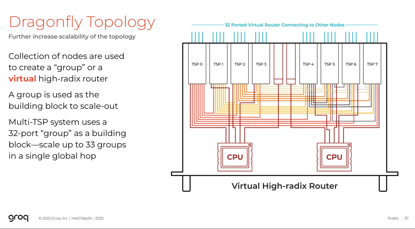
Remember how Mr. Abts would show up again? Yea, he sort of invented Dragonfly at Google.

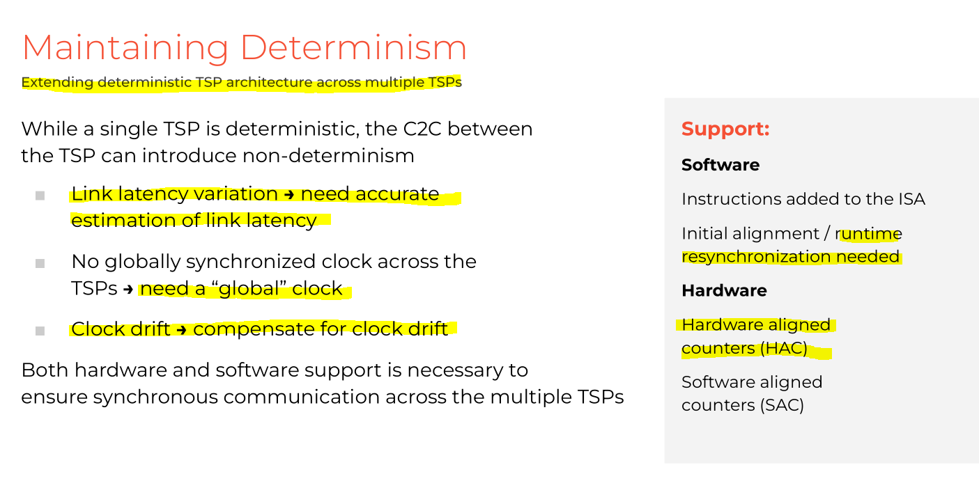
I have read their patents on how the sync works. There are much better ways of doing this. More on this in next section.
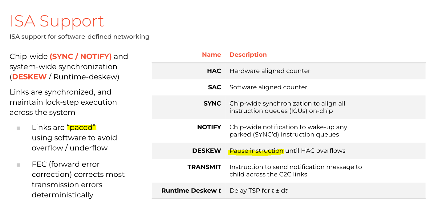
If skew varies over time (it does!) execution grinds to a halt by design.
This is true. Groq architecture places such an enormous burden on the compiler, a team of 10 competent digital designers could replicate the design in under 6 months.
Design of this chip is quite simple. Complexity burden is not gone! COMPLEXITY SHIFTS TO THE MOST HELLISH COMPILER IN THE HISTORY OF COMPUTERS.
Here are some snips from Groq patents.
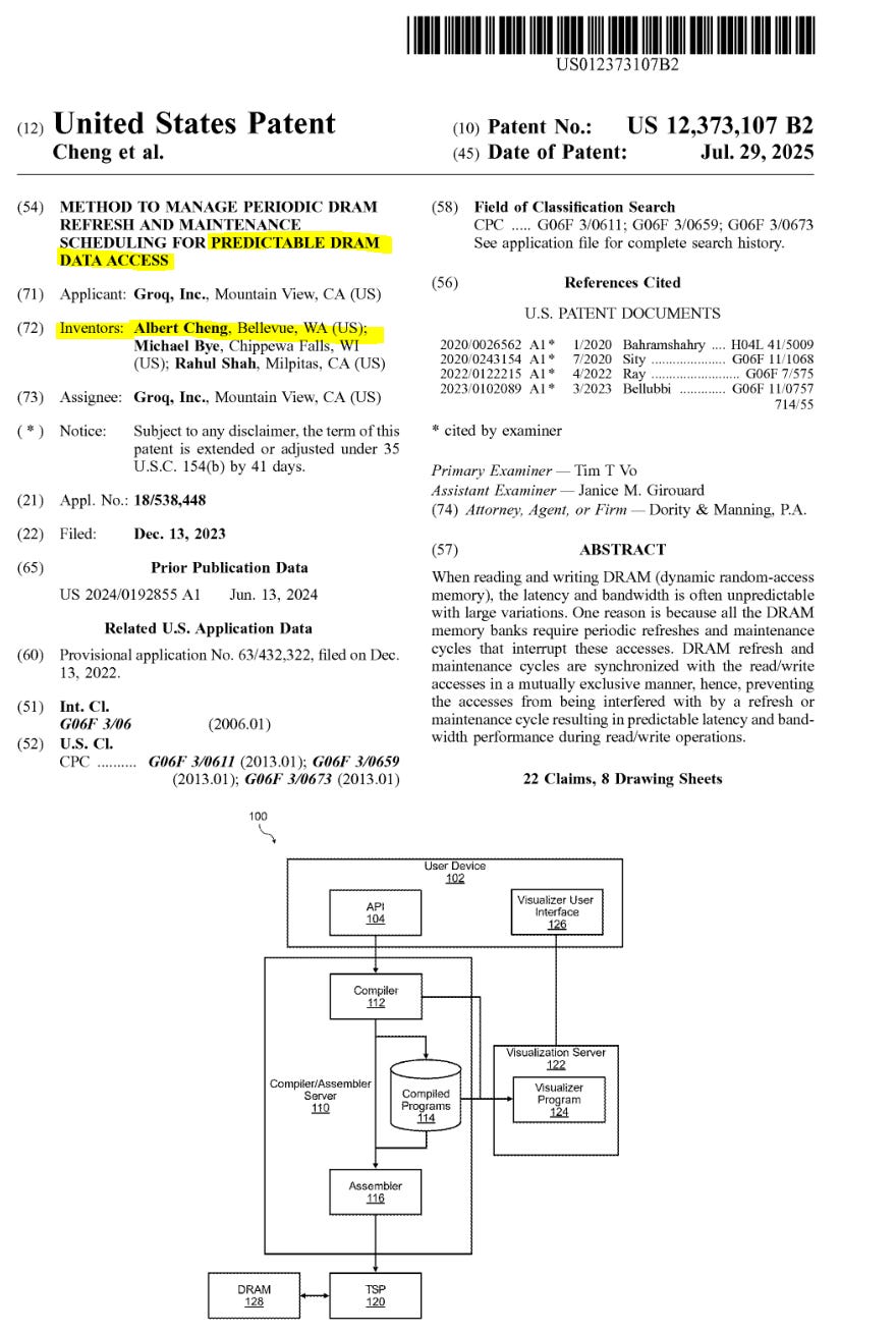
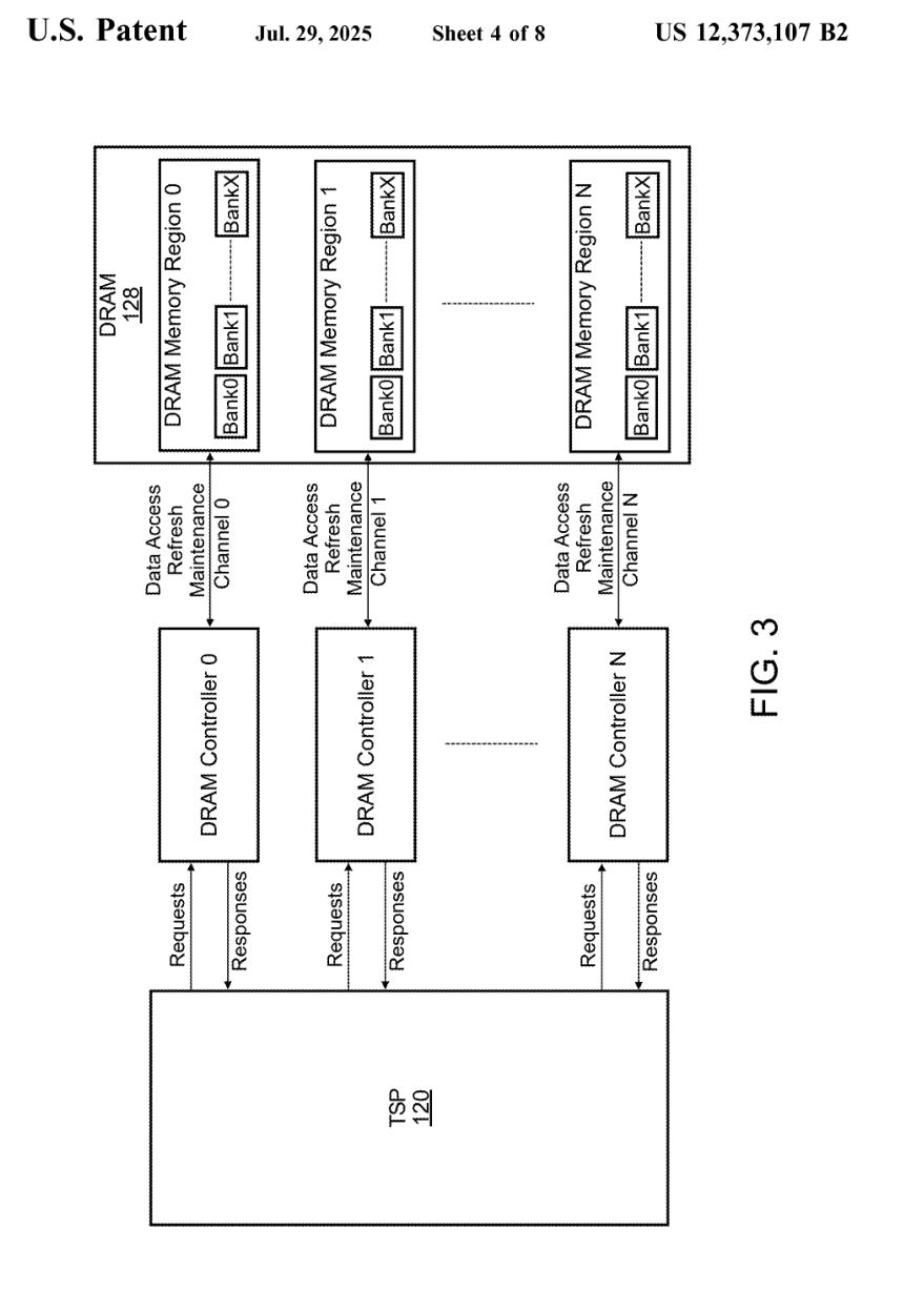
Mr. Abts left 3 years ago to join Nvidia. None of Groq’s chips use DRAM of any kind. Clearly this patent for making DRAM deterministic using scheduling packet tricks does not work. Otherwise, Groq would have added DRAM by now.
Here is a patent they actually use.
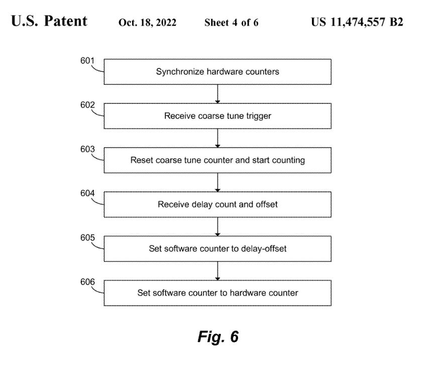
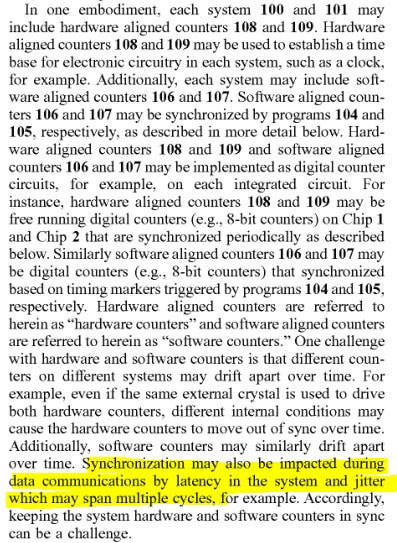
You’re damn right SerDes jitter and PPM drift of clocks will fuck over this counter-based sync scheme!
Groq is the most insane, unorthodox, violently imbalanced computer ever created. There is a reason why myself and many others have been shitting on this abomination of years!
But… after 6+ years of working on the compiler and running a money-incinerating inference cloud to learn how to make the compiler better… they seem to have figured out something.
Set aside your biases and assume the compiler is functional, or at least capable of becoming functional.
Imagine you are Nvidia and have all the IP needed to make Groq actually reach it’s theoretical full potential.
$20B is cheap. This is a transformative acquisition. Much bigger than Mellanox!
Let me show you how Nvidia is gona make Groq live to it’s full potential.
[6] Nvidia Incredible IP Synergies with Groq-Style Architecture
Taiwan rumor mill is already jerking off to leaks regarding PCB specs but this misses the point. Supply-chain degenerates have no clue what the real value of Groq is.
I frankly don’t give a shit what Nvidia/Groq cobbles together in the short term using Groq V3 chip. SF4X process node is worse than TSMC N6, and in some cases worse than N7 lol.
Groq architecture and Nvidia IP have incredible synergy. They are going to make something orders of magnitude better in 18 months.
[6.a] Clock-Forwarded SerDes
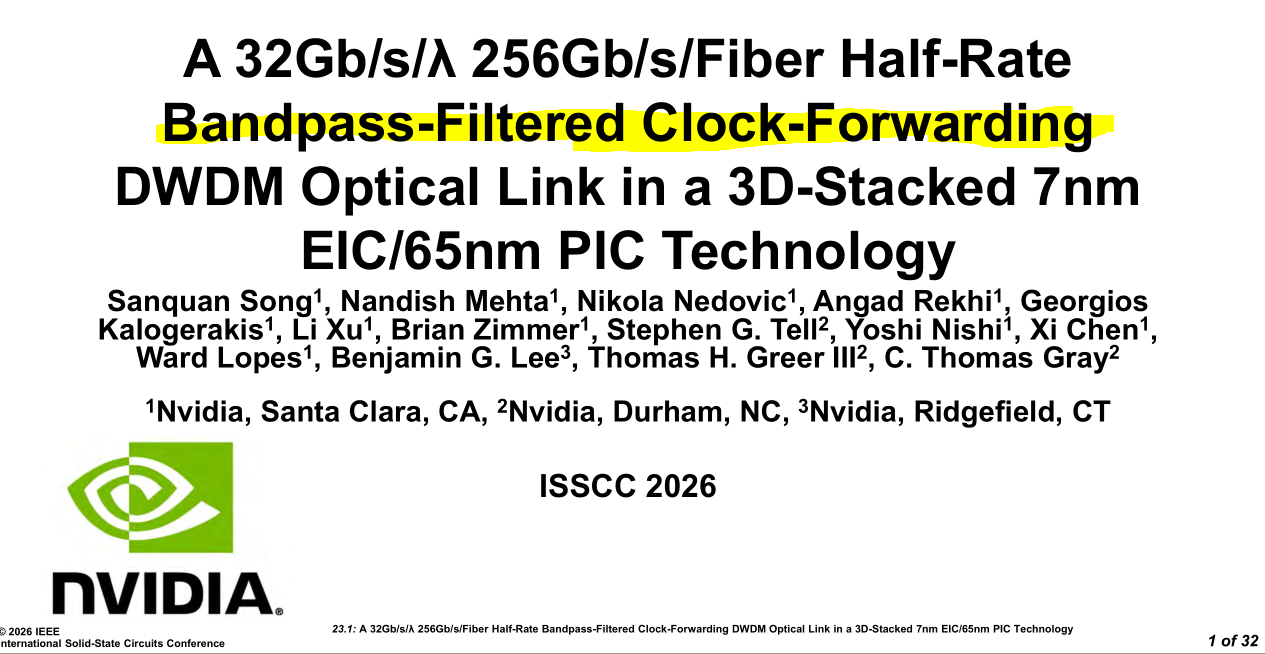
Nvidia just presented their optical clock-forwarded die-to-die link at ISSCC.
I have more detailed coverage here.

For this post, I will only re-cover the clock-forwarding section.
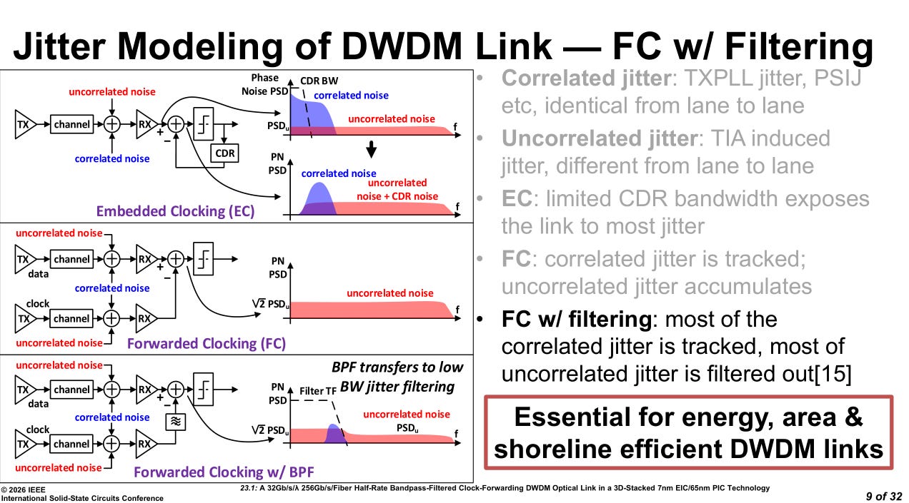
Designing this bandpass filter for the forwarded clock is very challenging. Lots of PVT sensitivity.
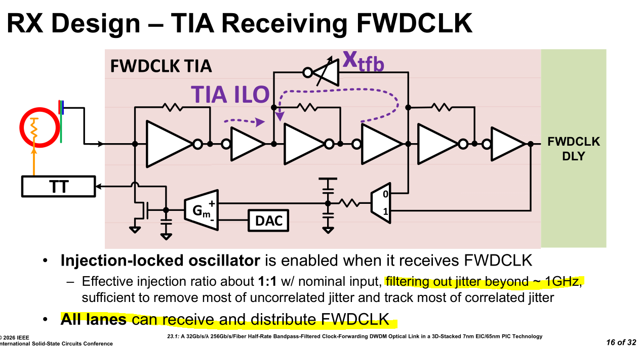
All lanes support receiving the forwarded clock in order to optimize yield. This burns a non-trivial amount of area. They must have had a performance reason to do this.
Perhaps electrical crosstalk severity varies across dice?
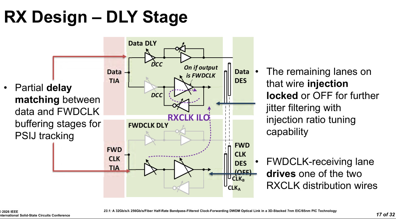
The delay matching circuits are rather complicated. Both clock forward and data lanes have multiple tunable delay elements. Variation over time (VT induced) is a huge problem. Injection locking is a key strategy.
https://en.wikipedia.org/wiki/Injection_locking

In short, injection locking uses a feedback path to re-enforce the primary target tone and attenuate/eliminate harmonics and other sources of sinusoidal jitter.
Injection locking leads to huge gains but the circuit is very difficult to tune.
Forward clock phase variation is ~0.5 UI (unit interval) or around 16 picoseconds.
I assure you that clock accuracy of under 16 picoseconds is way better than whatever Groq managed to achieve with their lame counter-based scheme.
IMAGINE HOW MUCH BETTER GROQ-STYLE HARDWARE ARCHITECTURE CAN PERFORM WITH REAL CLOCK FOWARDING OVER OPTICS!!!!!!!!!!!!!!!!!!!!!!!!!
[6.b] Hybrid Bonding
One obvious way to improve Groq-style architecture is to used hybrid-bonding to expand the SRAM scratchpad. You can get say ~2X capacity with minimal latency penalty using hybrid bonding offerings from TSMC or Intel Foundry. Groq did not have the resources to pursue this. Nvidia can handle this!
The latency penalties don’t matter anyway as the compiler needs to be deterministic and will just back out the delays ahead of time.
[6.c] Leading Thermal Team
One of the problems with a Groq-style architecture is thermal density. While the absolute power of the chip is not high, parts of the execution logic become very very hot.
Nvidia has one of the worlds best liquid cooling and thermal design teams. Thermal hotspots won’t be a problem anymore. I suspect Groq has to underclock relative to their targets due to hotspots. Easy fix but leaves performance on the table.
[6.d] Theoretical Optical Global Clock
Nvidia’s optical clock-forwarding IP is sensitive to chromatic dispersion.
This is surprising.
https://www.rp-photonics.com/chromatic_dispersion.html
 Means in Fiber Optics")
Chromatic dispersion is an optical phenomenon that widens signals in frequency domain. The DSP way of fixing this is to simply over-sample.

Chromatic dispersion is typically a problem for long-haul C-band links. O-band usually does not care about this.
That is why I am so surprised. Nvidia is on O-band and intuitively this would be a non-issue. Clearly, their system is extremely sensitive!
This indicates that Nvidia’s optical clock-forwarding IP has limited reach. Let’s say within a rack only.
If it were possible to distribute a global optical clock across racks within an entire datacenter… that would be fucking amazing for Groq-style architecture.

Optical atomic clocks have a rich history, in laboratory and research applications.
https://en.wikipedia.org/wiki/Optical_clock
Recently, this tech has gotten renewed interest for datacenter.
It really is possible. Nvidia optics group is galaxy-brain. They can do this!
For all these years, Groq compiler engineers have been using lame hacks and software counters to achieve mediocre symbolization. Nvidia has the unique IP needed to fulfill Jhonathan Ross’s wildest dreams and truly unlock the insane potential of the worlds most imbalanced computer.
[7] Mock-Up of Possible Nvidia/Groq Product
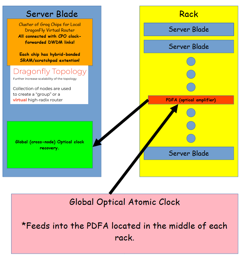
[8] Any Idiot Can Build a Bridge // Golden-Age for Unhinged Computers
<todo>
overview modern altera fpga
sn mercy killing
wait no I want to live
explain unit interval
use nvidia ISSCC paper again
spectrum of unhinged
brittle architecture spectrum
groq cannot integrate. must be on island?
assume existance of some AI workload that can run on island
supply chain angle
any idiot can build a bridge analogy
happy for everyone
even cerebras
congrats gif
bridge made of WSE
insult hardware gaps
Gotta admit - as a casual reader, I do not have the mental context to appreciate the scope of what, "REAL CLOCK FOWARDING OVER OPTICS!!!!!!!!!!!!!!!!!!!!!!!!!", implies.
Fun enthusiasm, though
Thanks for sharing. There is another start up called Tensordyne which is about to reveal their tape out in April. Tensordyne uses logarithmic math turning expensive multiplications into simple additions and thereby simplifying the data flow/making it more efficient/faster. Tensordyne is positioned as a purer, more radical version of the dataflow future Nvidia is buying. While Nvidia is integrating Groq’s deterministic networking to save its dominant position, Tensordyne is betting that even a "Groq-ified" Nvidia will eventually be too power-hungry compared to a system that combines dataflow with logarithmic math.