

Irrational Analysis is heavily invested in the semiconductor industry.
Positions will change over time and are regularly updated.
Opinions are authors own and do not represent past, present, and/or future employers.
All content published on this newsletter is based on public information and independent research conducted since 2011.
This newsletter is not financial advice and readers should always do their own research before investing in any security.
Feel free to contact me via email at: irrational_analysis@proton.me
Two years ago, I attended Hot Chips in-person for the first time and somehow had the opportunity to meet one of my heroes, Jon of Asianometry. For some reason he gave me a shout out and overnight my subscriber count doubled.

It’s crazy how much has changed in the last two years. And yet, some things have not changed. There is still one conference that stands above the rest.
🌶️ Welcome to the Irrational Recap of Hot Chips 2026! 🌶️
Contents:
Memory
HBM: High-Bandwidth Mistake
D-Matrix
HBF Analysis: Niche but how big?
Samsung LPDDR5X-PIM: Intrinsic Bad Idea
Networking
Broadcom Thor Ultra
Nvidia BlueField-4: The Neocould NIC
Nvidia Spectrum-X Multiplane
AI ASIC
Meta: Worst of Both Worlds (Rec and GenAI)
Nvidia/Groq Rubin/LPU Disagg
Cerebras
Microsoft Maia is still dogshit and embarrassing.
Sambanova: Still Alive After Almost Euthanasia
Google TPU V8
OpenAI Jalapeno
GPU
Nvidia Rubin
AMD MI400
Intel Xe Zombie (please put them out of their misery)
Waymo
CPU (real ones not RISC-V garbage)
IBM Galaxy-Brain Dual-ISA Mainframe-Grade CPU
Nvidia Vera (is not complete garbage like Grace)
Intel Dimond Rapids
ARM First-Party CPU
Fujitsu Monaka
Roast of RISC-V
Miscellaneous
AMD/Xilinx RF FPGA
Opticore
Chat with Ashkan (Photonics God at AMS OSRAM) on VCSEL CPO/NPO
Chat with Stevan, President of Olix, on pure SRAM machines.
The legend of Jeff from Etched.
Higher-Level Takeaways
Multi-Vendor Disagg Inference Is Temporary
AI acceleration of chip design is real but not in the way the cultists want you to believe.
DRAM vendors have overplayed their hand.
Full Portfolio Update: 9/5/2026
[1] Memory
This subject was a strange overhang. Difficult to explain so perhaps a quick side story would help.
On the first day one of the Hot Chips staff was giving the usual shout out to sponsors. Loose quoting here…
“And thank you to all out sponsors who help us keep ticket prices low. In fact this year we did not need to raise ticket pricing…..
So its great you get to save money on the ticket to buy more memory…”
The energy in the room was weird.
[1.a] HBM: High-Bandwidth Mistake
I feel vindicated on this post.

All three DRAM giants presented on HBM. Most of it was almost defensive.
“Let’s remind them how great HBM is even though everyone is staring daggers at us and asking for de-spec.”
Let’s start with Samsung, who focused on the HBM base die and reminded me why I own a good amount of their shares in a long-only account.
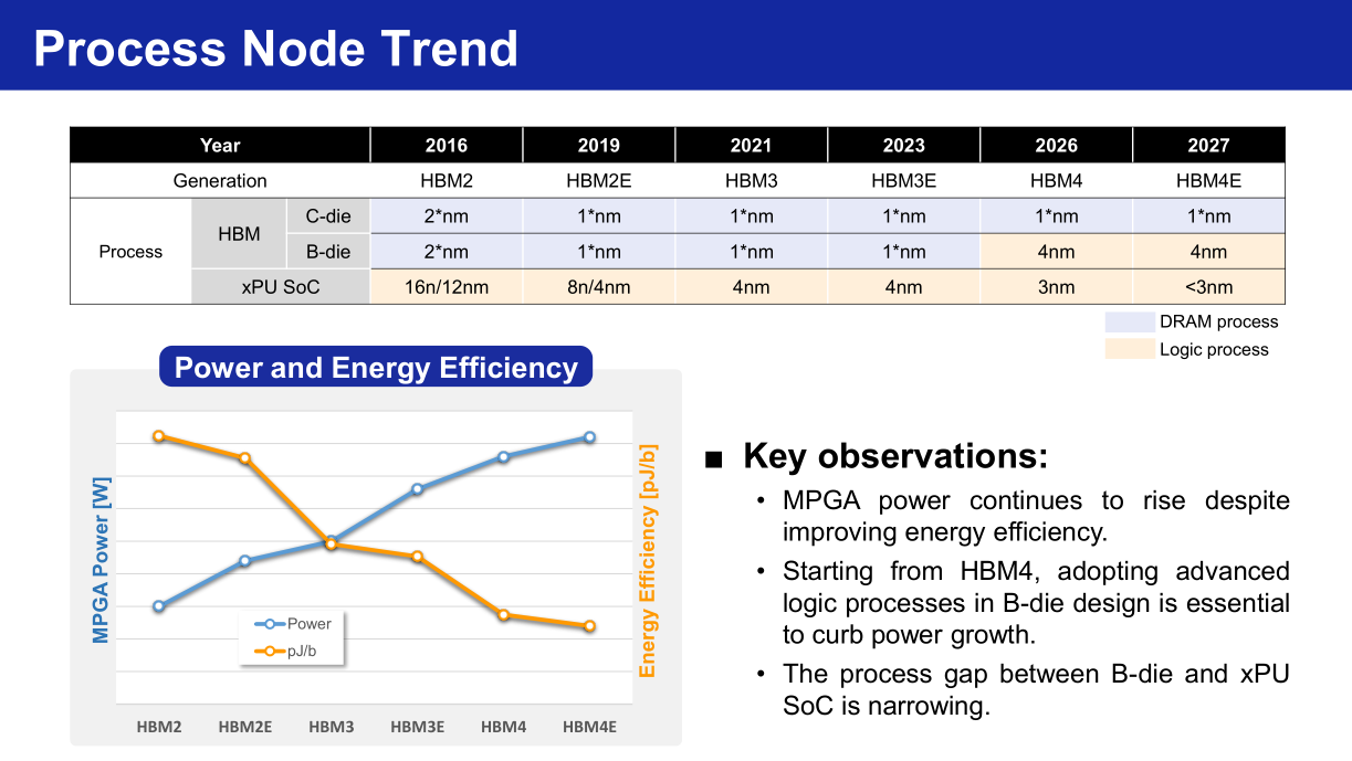
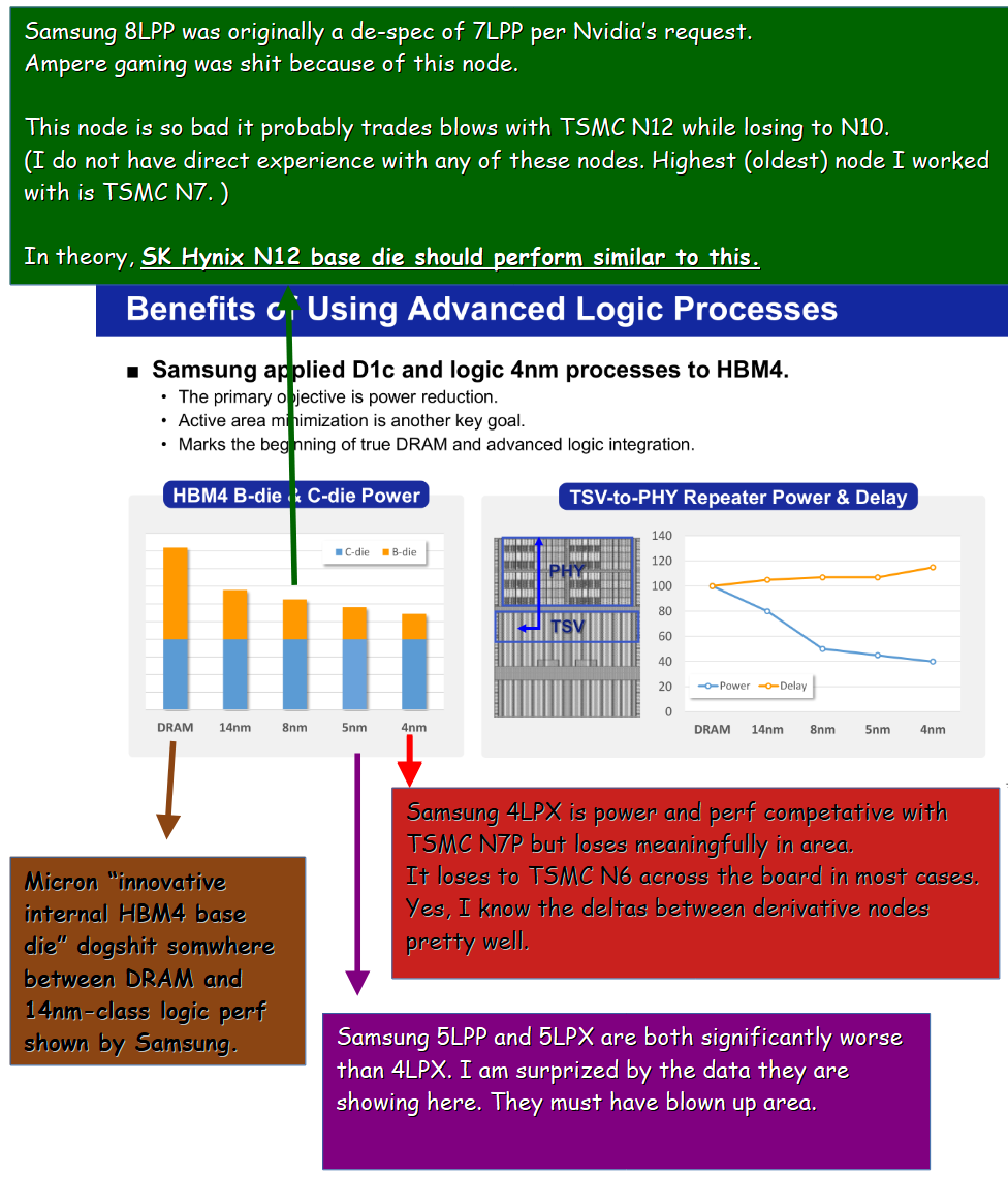
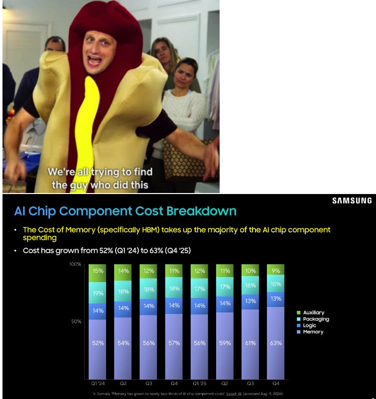
Thanks Samsung for showing clear data.

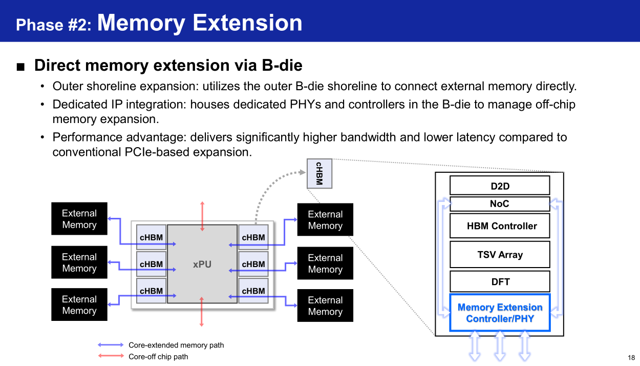
There are a lot of slides but frankly redundant. Also everyone already knows this.
HBM logic base die going forward are going to be much better because:
Use a real D2D PHY (UCIe, NVLink D2D, Broadcom MAX, Marvell 64G bidi D2D, Elyian) instead of the dogshit PHY JEDEC retards came up with.
Move controller to free up area on main ASIC.
Add an extender D2D PHY (electrical or optical) to access even more memory because HBM TSVs determine shoreline requirement per stack, not the stupid HBM PHY. In other words, the D2D is going to be significantly over-subscribed. Might as well use that bandwidth for other things.
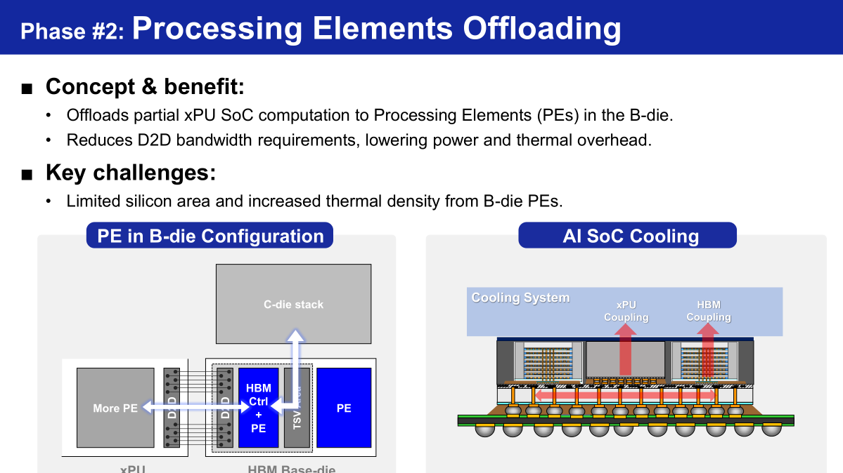
Compute offload to HBM base die is a terrible idea and nobody should be stupid enough to try this.
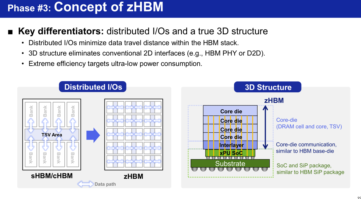
This is conceptually similar to what D-Matrix is trying to do. Will come back to this in their section.
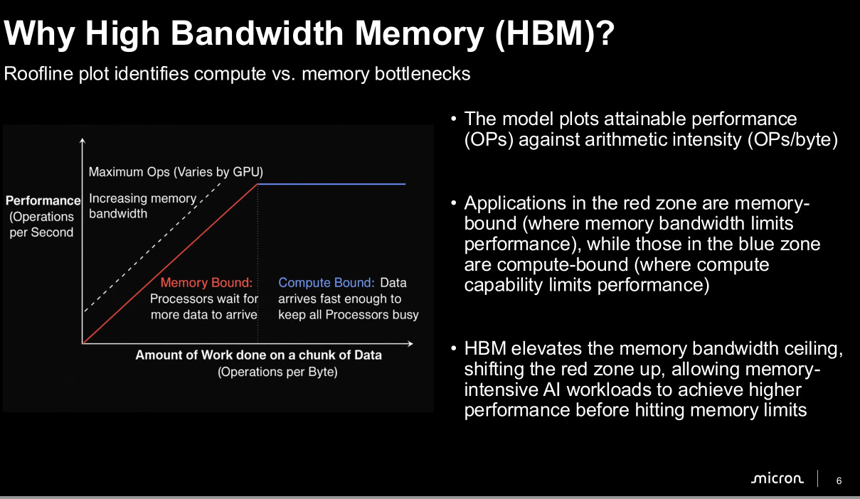
Micron presentation boring.
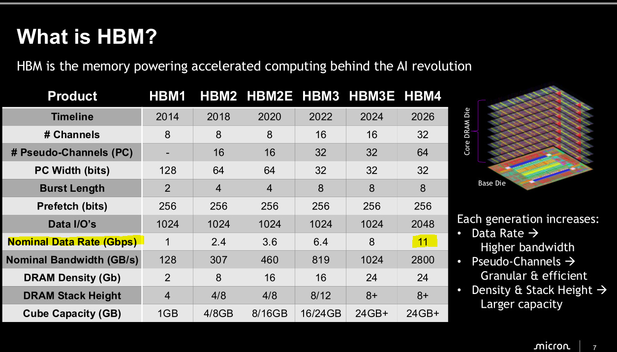
Bold move putting the datarate only Samsung can reliably achieve in your table.
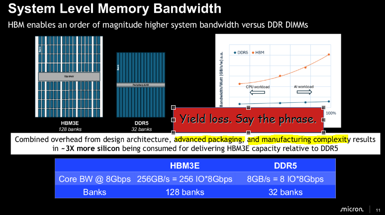
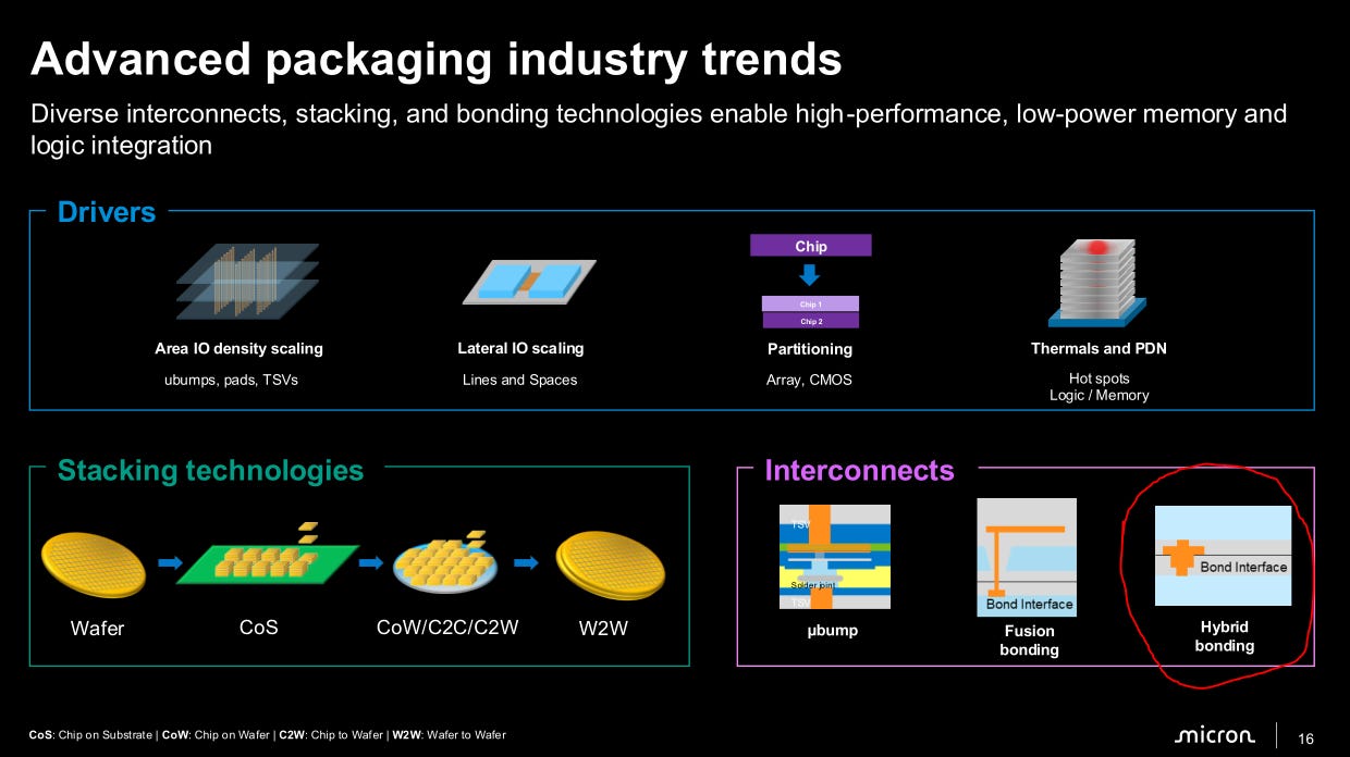
Given the de-spec trend, hybrid-bonding is fucked and that means BESI. I liquidated entire position and re-allocating to other things. Mostly EU and Japan optics.
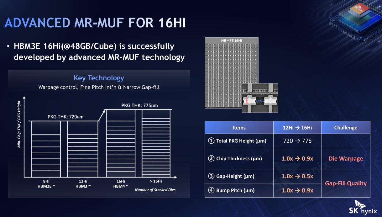
Again everyone looking into de-specing from 12-hi to 8-hi or even 4-hi.
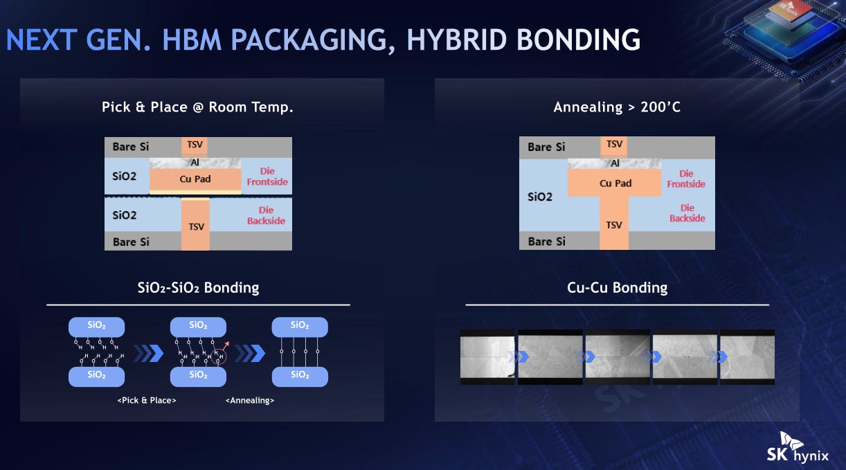
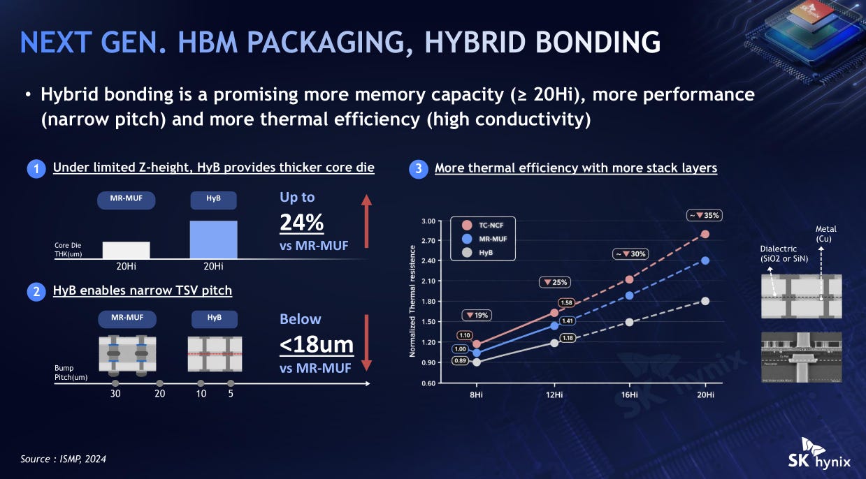
8-hi does not need hybrid bonding. 12-hi I feel should have used hybrid bonding but all three vendors managed to figure it out to some extent.
RIP BESI lmao.
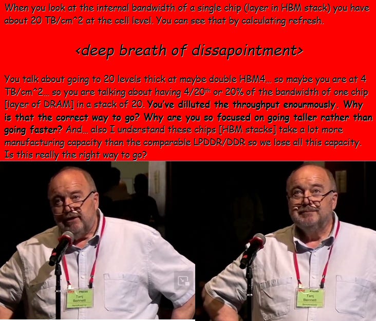
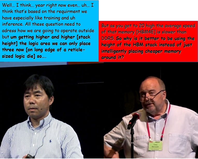
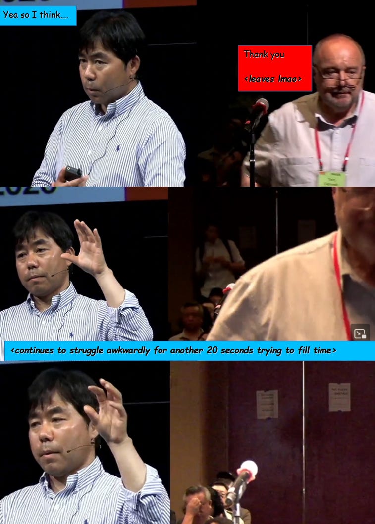
And now we arrive to the highlight of this conference, Tanj absolutely roasting SK Hynix. Me and Tanj agree on this topic.
HBM: HIGH BANDWIDTH MISTAKE
[1.b] D-Matrix
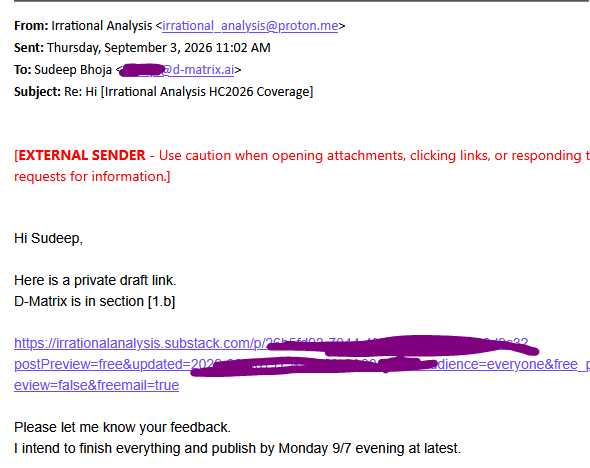
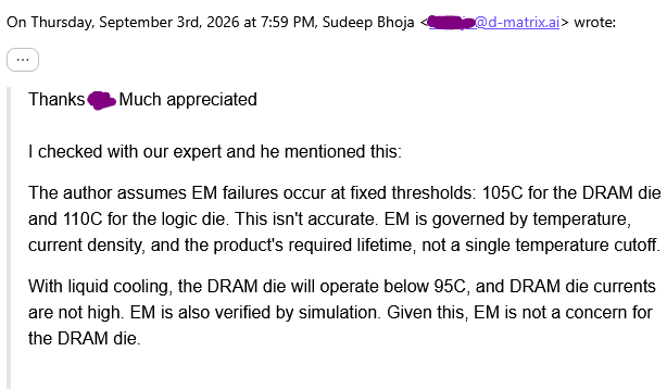
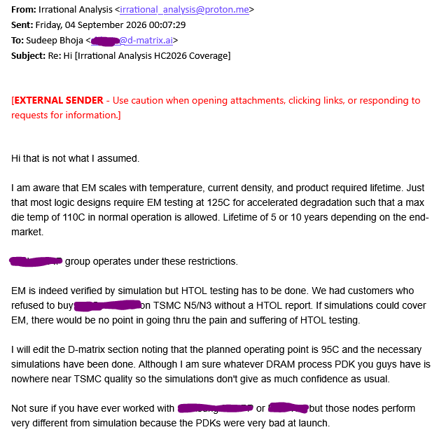
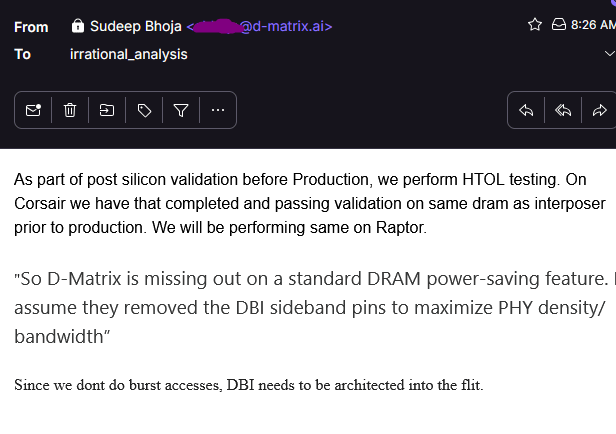
Note: A private copy of this section was shared with Sudeep for feedback. No opinions were changed. He asked nicely at lunch to give feedback and make his case.
Here are the emails so you can see for yourself.
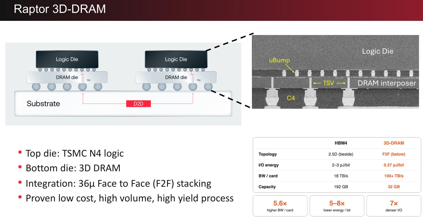
D-matrix is first to real 3D-DRAM. Cerebras, Nvidia/Groq, and Fractile are all working on something similar in spirit, but D-matrix is the first with real test chips.
For now, D-matrix has chosen 36-micron micro-bump packaging, which is less dense than the 10-micron bump pitch HBM uses. There is a future option for hybrid-bonding but it looks like they chose to be conservative on Raptor given the significant complexity everywhere else in the system. This is glorious engineering.
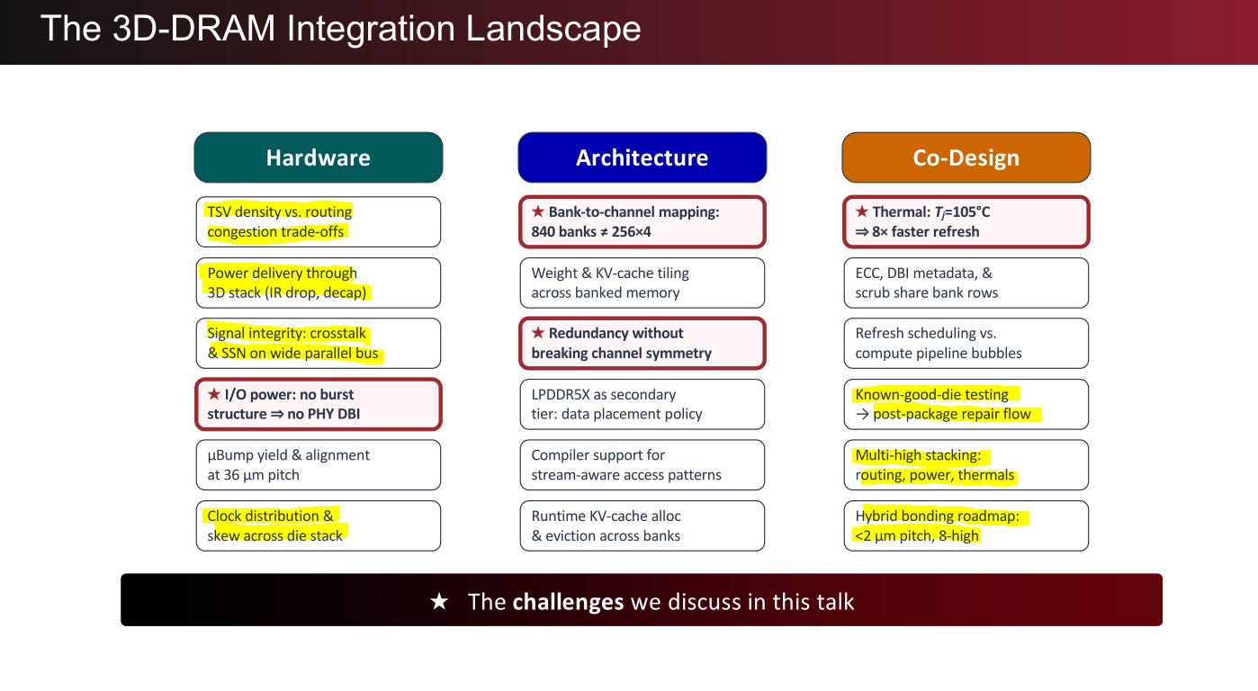
There is so much cool stuff that did not make it into this presentation and I would love to cover it in the future. For now, we only have the red boxes.
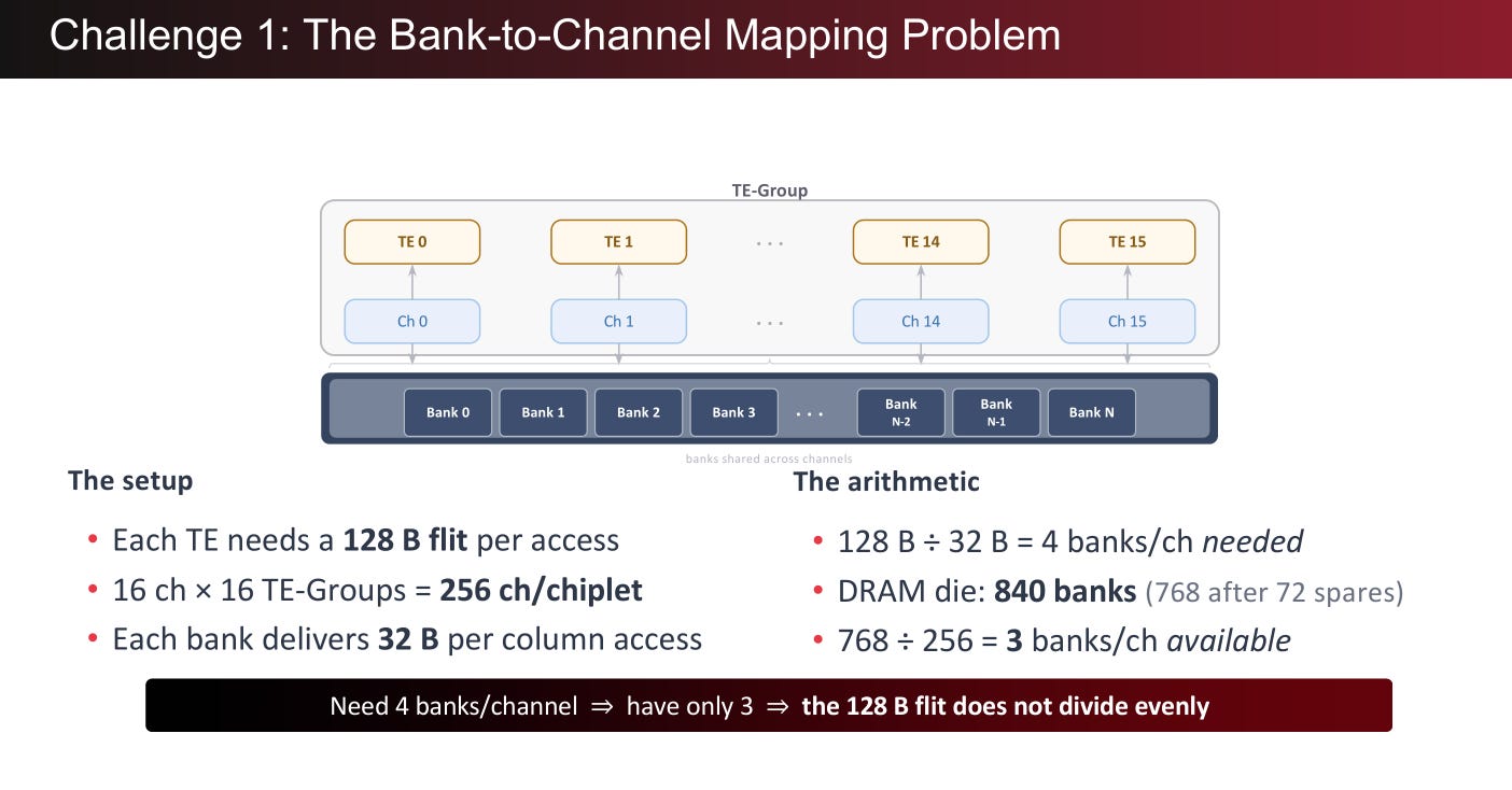
D-matrix compute (tensor engine aka TE) is designed around a 128-byte data access. The problem is they only have three d-ramm banks per channel which leads to a 96-byte read.
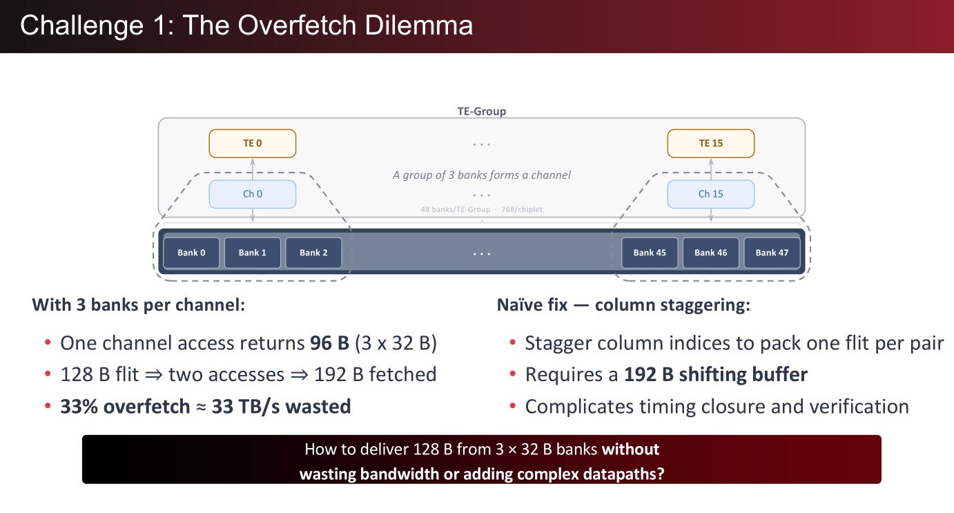
The dumb solutions either waste 33% of PHY bandwidth or create complex shifting digital logic.
Which raises the obvious question… why does this problem exist? D-matrix controls the TE design and the custom DRAM design. Why not make 4-bank per channel DRAM or reduce TE size such that it accepts 96-bytes?
Here is the full ISCA paper.

And here is a clue.
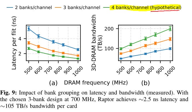
I suspect their original plan was for 4-banks per channel and something prevented that design goal from being achieved in Raptor. Maybe next gen.
As for why not make the TE 96-byte based, they probably already have a lot of compiler stuff designed around 128-byte and 96 is not a power of two so that would lead to annoying problems.
So how to solve this?
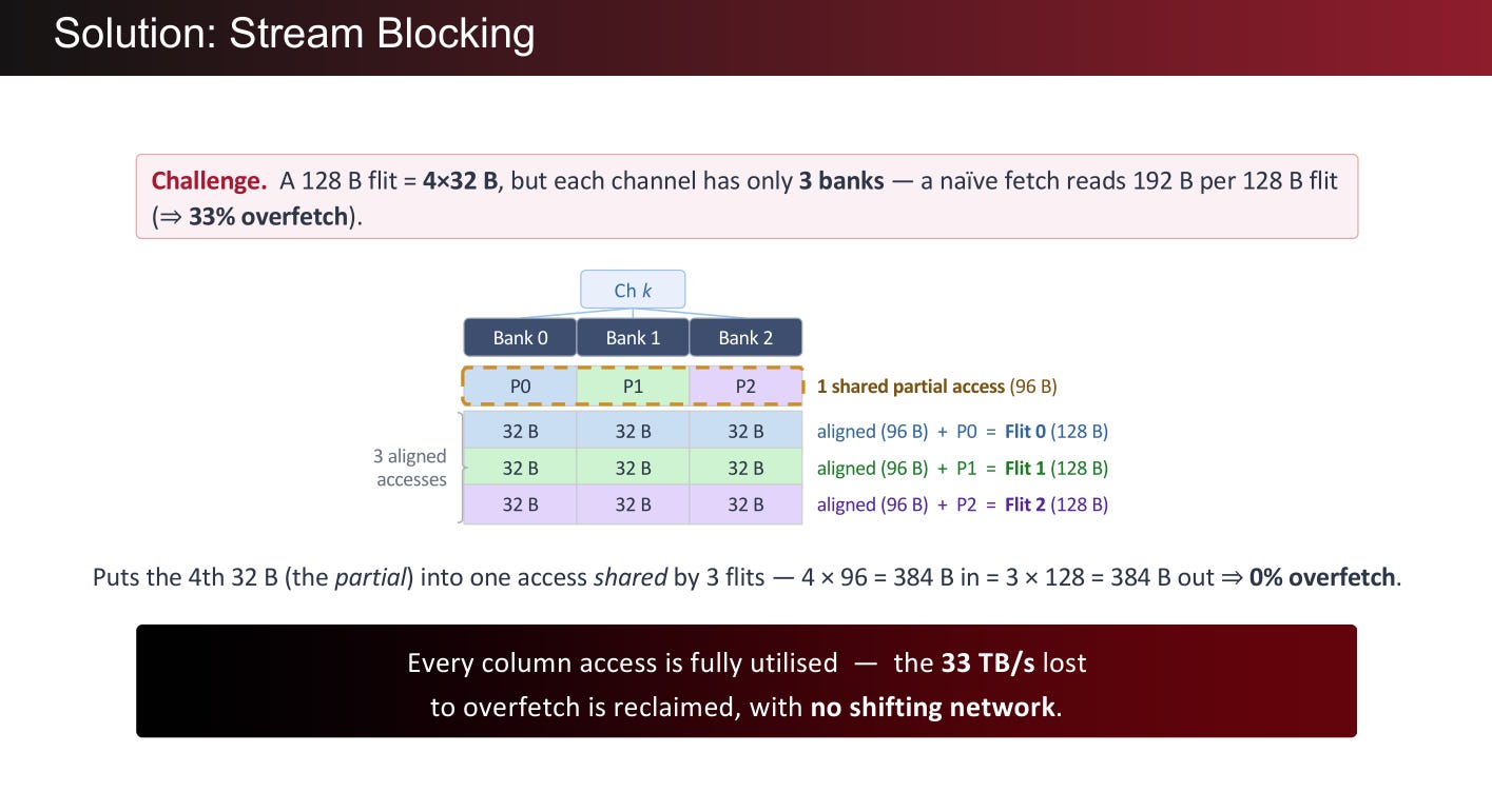
To me, it looks like some registers in the logic die area dedicated to holding multiple FLIT (reads). Probably wastes a small amount of logic die area and power but leaves the digital logic complexity low compared to a shifting network. Curious on the PPA delta between this stream blocking thing and a shifting network.
DRAM (HBM and regular DDR) has a feature called DBI, data-bus inversion.
https://www.rambus.com/chip-interface-ip-glossary/dbi/
Ideally, you want to minimize the number of bits that get flipped across FLITs. Flipping bits burns power. DBI is a strategy that uses a sideband (extra control bit) in the PHY to indicate if the associated FLIT is (intentionally) inverted.
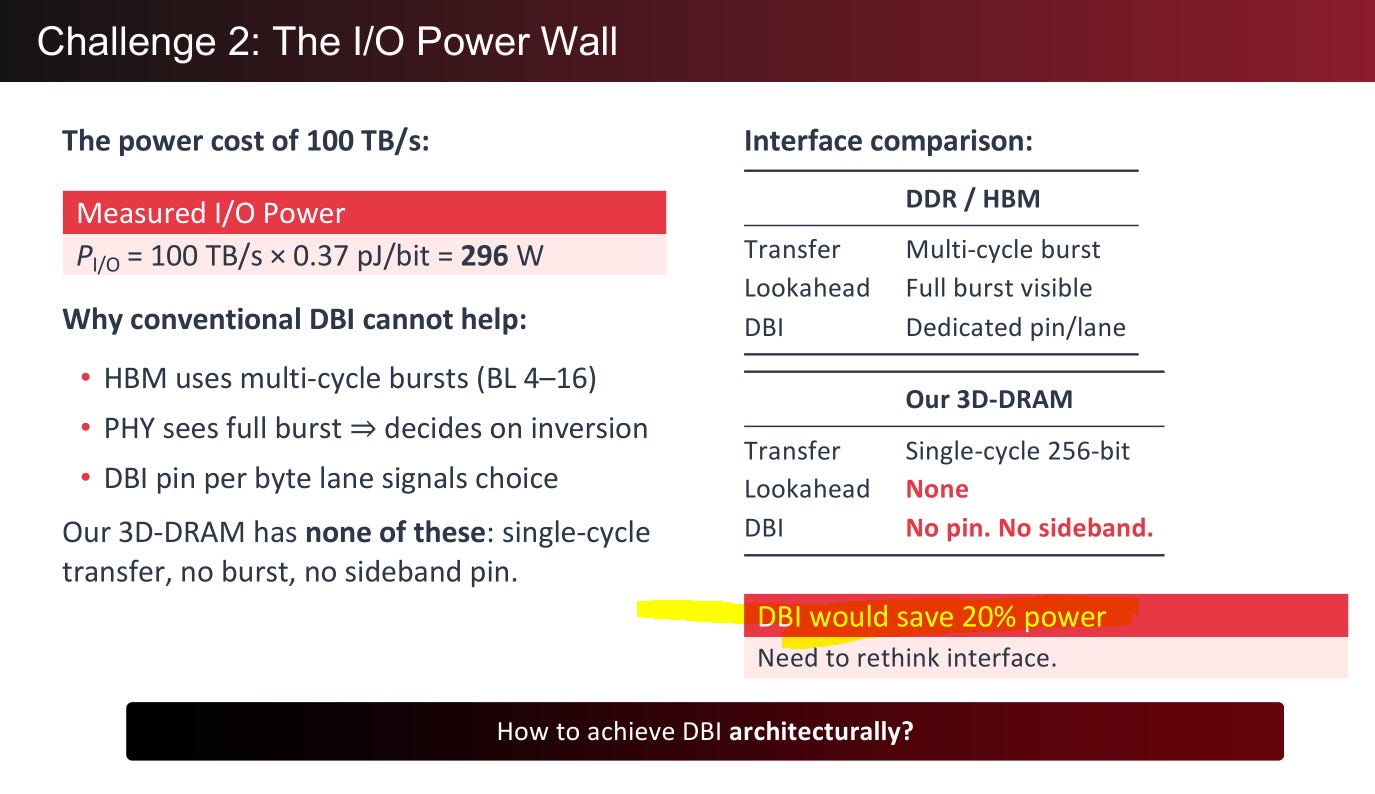
So D-Matrix is missing out on a standard DRAM power-saving feature. This is because D-matrix does not use burst accesses.
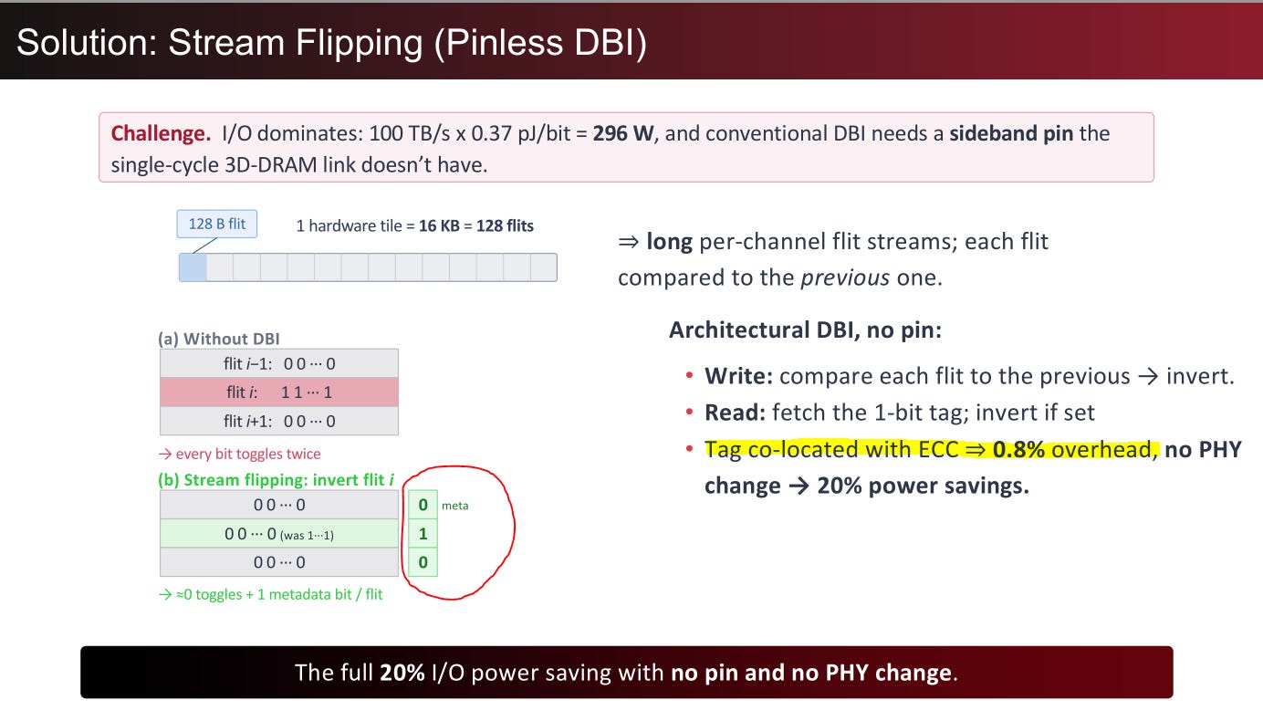
They encode the DBI pin info into the FLIT itself. This is a great solution.
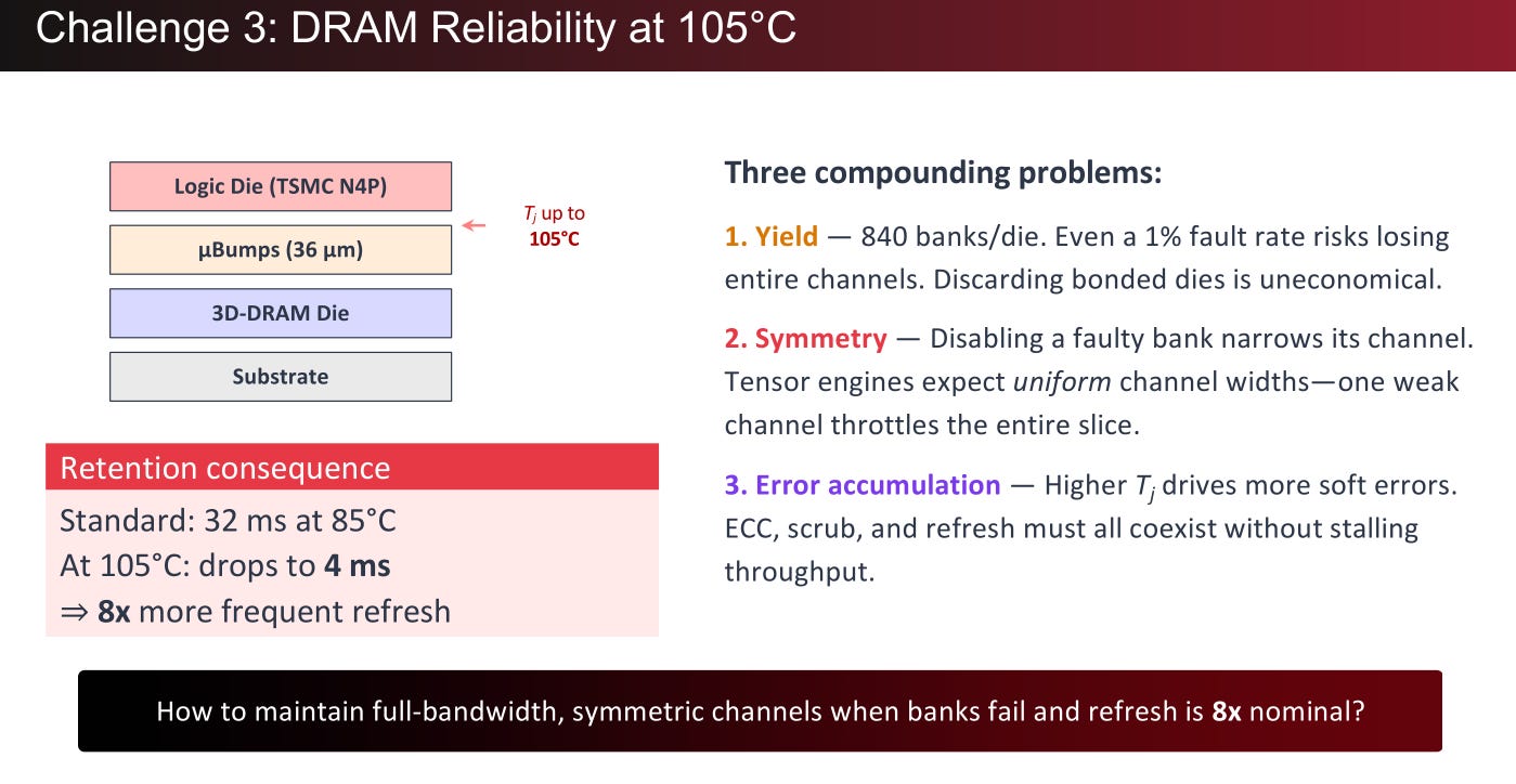
There are many forms of reliability.
D-Matrix is discussing reliability from the “does DRAM hold data reliably”. My main concern is electromigration. Will circle back to that.
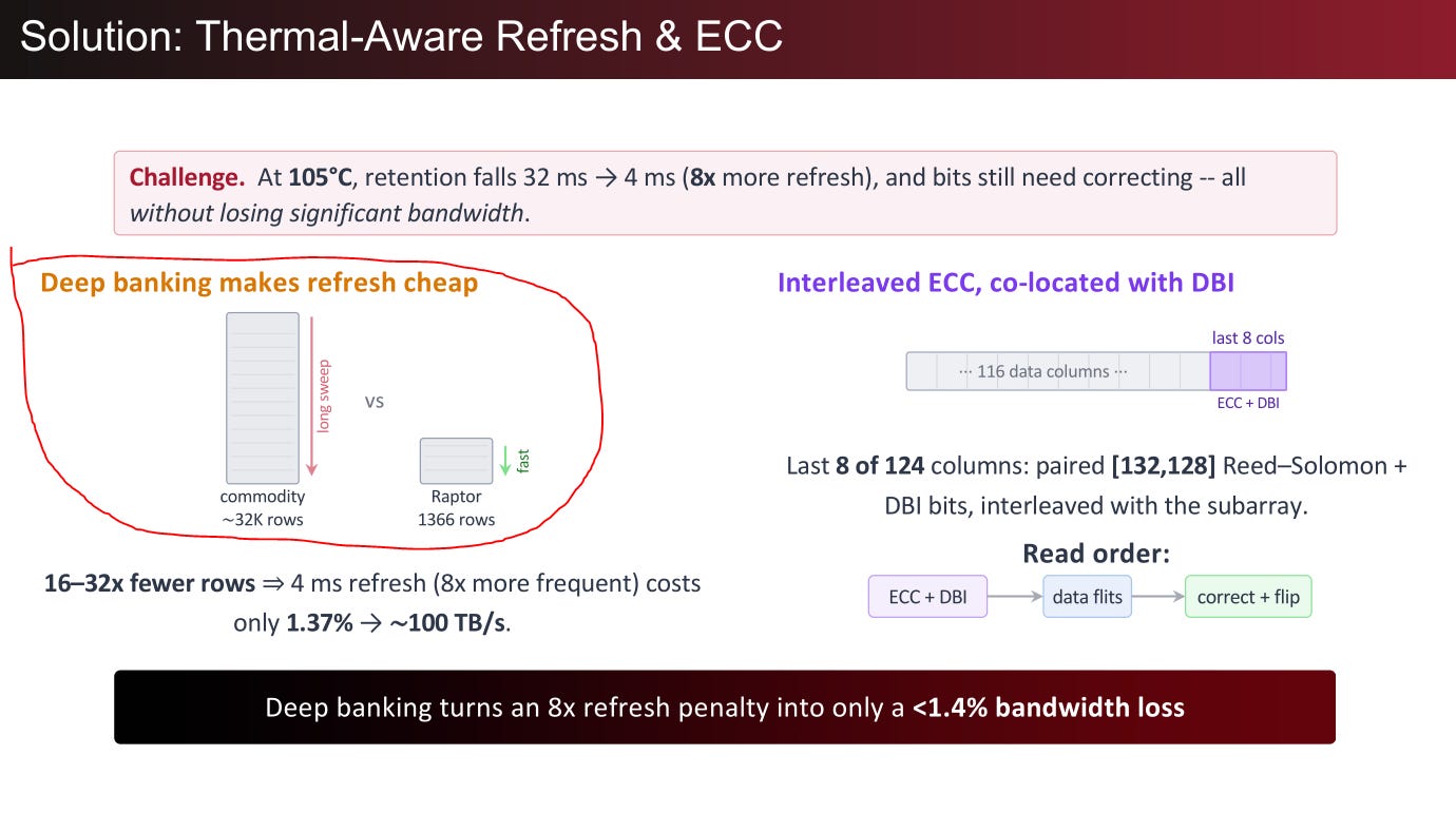
Presumably deep-banking sacrifices capacity compared to commodity DRAM. For the ECC, I am not sure why they chose Reed-Solomon. Usually for small packet sizes a simpler FEC such as BCH is used.
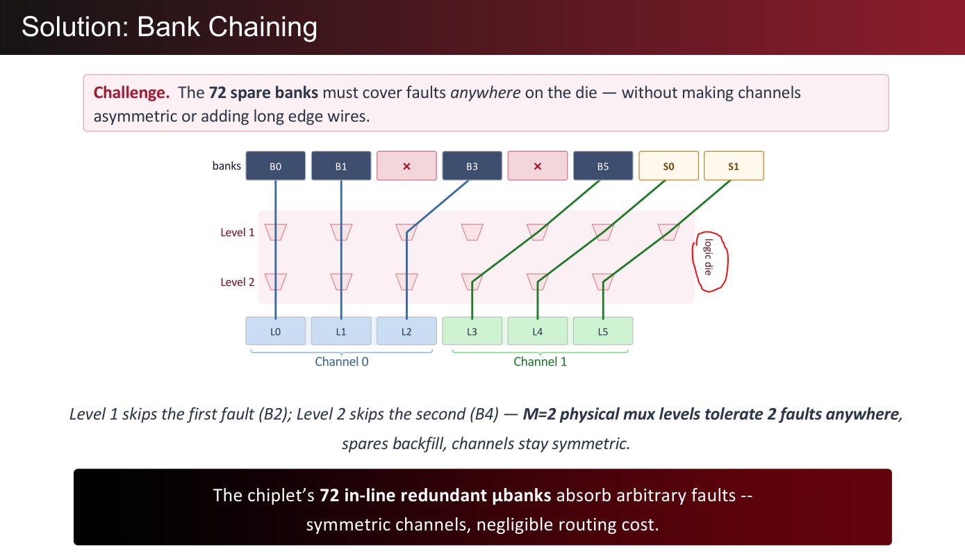
On the logic die there is a mux-tree to allow for defect recovery.
I am a huge fan of D-Matrix and greatly respect Sudeep and the entire team over there. A lot of incredibly interesting and well-done engineering.
There is an open question though and that is operating-life reliability.
All silicon designs undergo a test called HTOL, high-temperature operating life.
https://en.wikipedia.org/wiki/High-temperature_operating_life
The maximum “safe” operating temperature of a chip is determined both by the PDK and the design itself. Typically, leading-edge logic designs have a max safe operating die-temp of 110C. This is generally true across all modern TSMC, Samsung Foundry, and Intel Foundry logic nodes.
In order to make sure your chips wont die early in the field, an accelerated-degradation test is needed. The numbers change depending on project but the following general procedure for HTOL testing is true. I have done this before it is not fun.
Take a sample lot of 60-180 devices and measure each device performance and current draw across every single power rail at room temperature, nominal voltage all rails.
Place devices into an oven. Set oven temp such that every device is at least 125C die temp while every single power rail is at +10-20% voltage.
Monitor all device functional performance (is it still alive) and current draw of all voltage rails. Typically using a shared PSU supplies all chips per rail for VDD, VDDH, …
Cool-down and test all devices at room temperature, nominal all rails at each of the following checkpoints. 48/168/500/1000 hours.
If at the end of 1000 hours of accelerated degradation all devices alive, performance roughly same as beginning, current draw all rails roughly the same, congrats you passed.
1000 hours is ~43 days. HTOL typically takes 2-3 months because thinks go wrong. Annoying problems like the test PCB cracks, power outage takes down the testing setup.
Broadly, all 3D DRAM efforts (D-Matrix, Fractile, Cerebras, Nvidia/Groq) scare me because DRAM process nodes were never designed for this level of abuse. Standard server DRAM sticks are rated for up to 80-85C die temp.
So if “max safe temp” of logic is 110C and for DRAM is 85C, what happens when you run DRAM at 105C?
Edit: D-Matrix claims the final operating point of Raptor’s DRAM die will be at 95C due to enhanced liquid cooling. They also state that EM simulations have been done (standard practice) and Raptor will undergo HTOL testing before production (also standard practice).
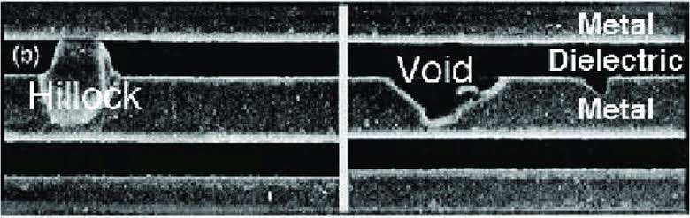

This is what electromigration (EM) looks like. Random short and open circuits all over the place.
In discussion with Sudeep, the previous version product (3D stacked but DRAM die only acts as a passive de-cap element), had “some problems but was fixed”.
Well this Raptor system is much higher risk. Electromigration is a very dangerous problem for D-Matrix Raptor (and all other 3D DRAM efforts) and only HTOL testing can prove otherwise.
[1.c] HBF Analysis: Niche but how big?
Perhaps the most well presented talk of the conference. Really enjoyed this one.
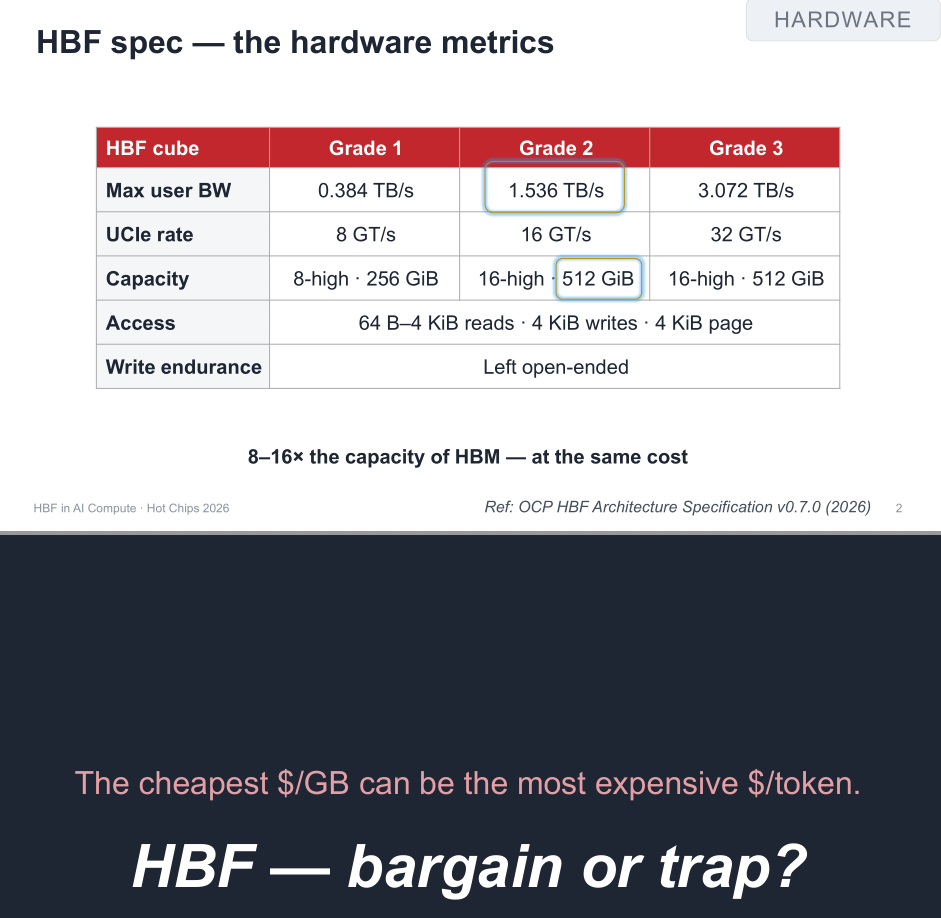
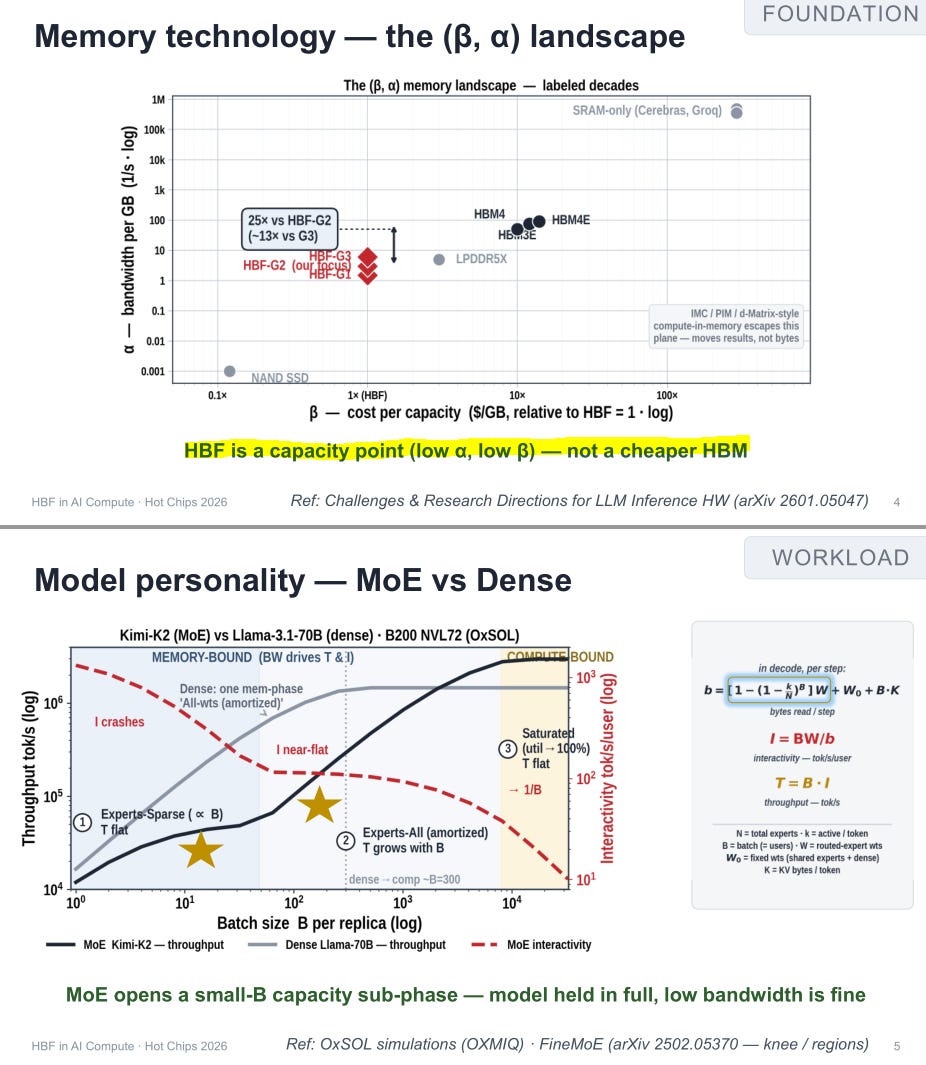
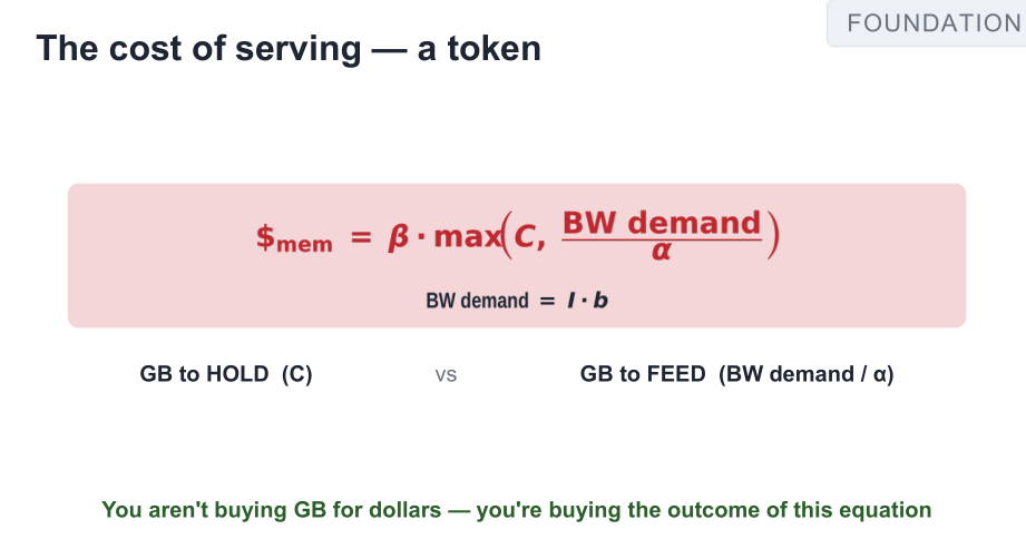
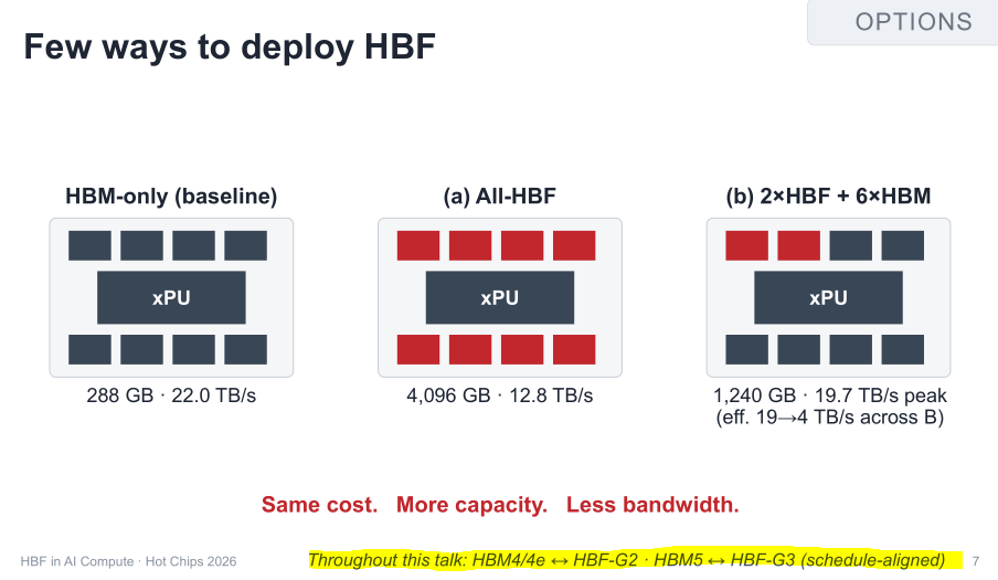
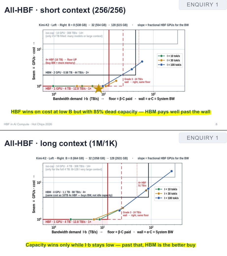
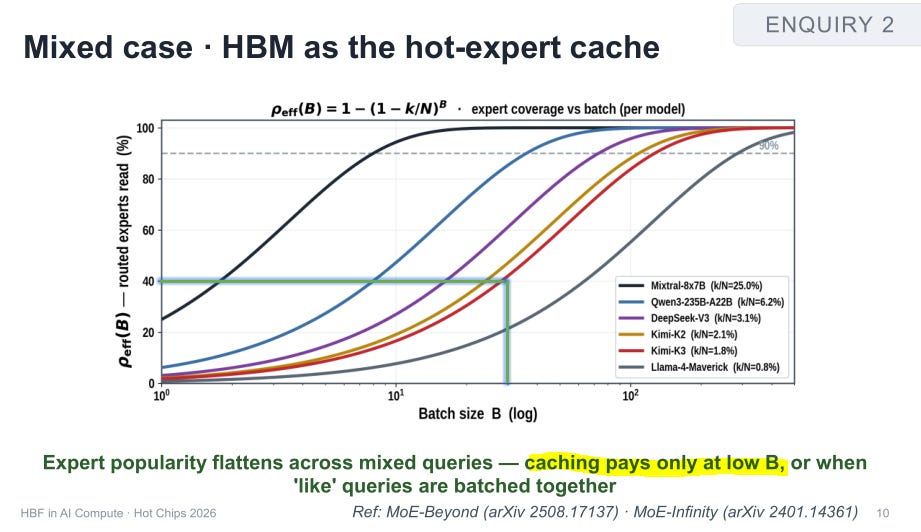
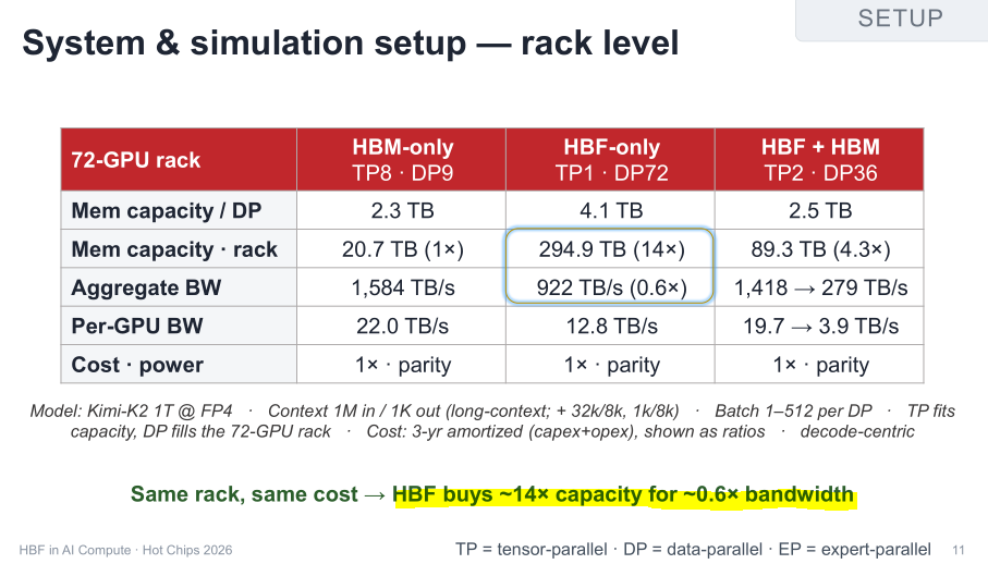
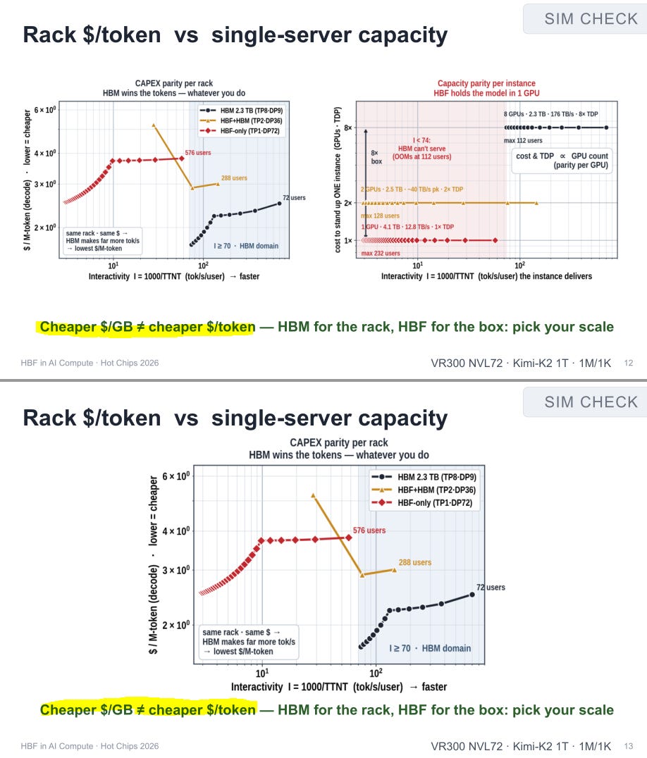
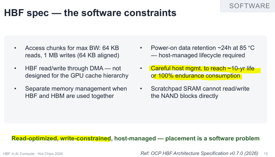
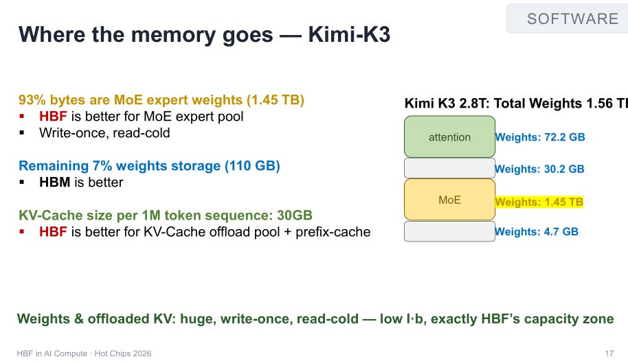
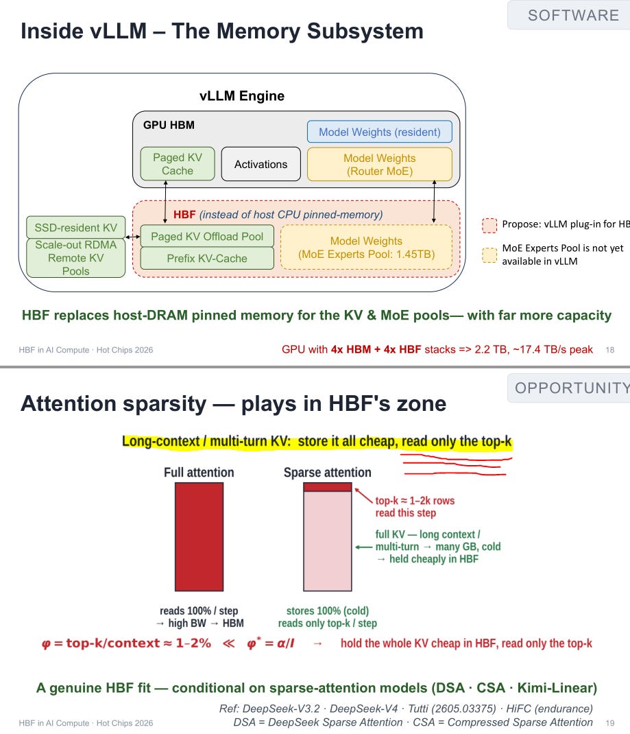
This scenario is the niche that matters economically for HBF.
Long-context + multi-turn KV
I have no idea how to size this niche market.
Also a lot of their assumptions were for low-active-param ratio. Anthropic models are comically high active param so that would help HBF case to an extent.
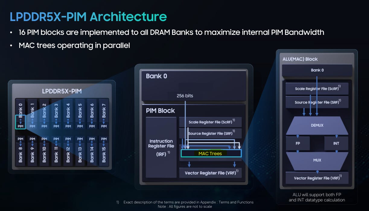
[1.d] Samsung LPDDR5X-PIM: Intrinsic Bad Idea
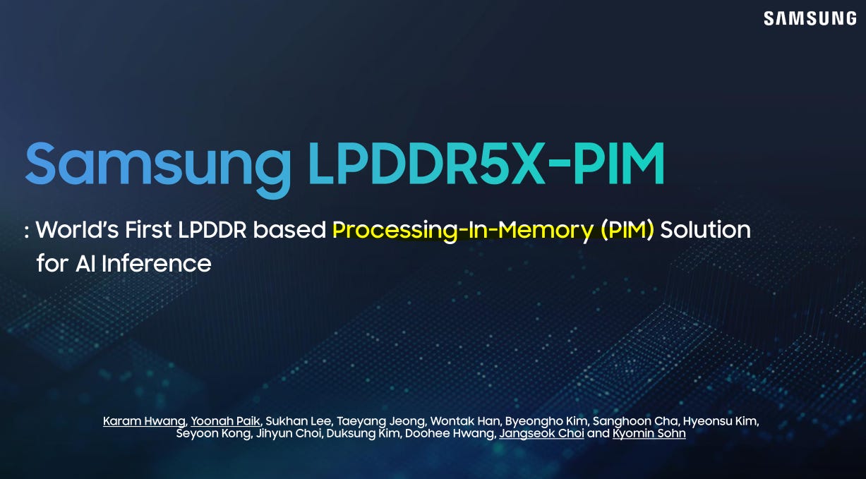
By default I hate all compute-in-memory AKA processing-in-memory strategies. It’s very simple…
Transistors in a DRAM process node are going to perform significantly worse than transistors from any reasonably modern (TSMC N6 equivalent or lower) logic process node.
Spending DRAM die area on compute reduces memory capacity.
This is a solution looking to solve the wrong problem. THIS IS AN I/O PROBLEM FIX THE REAL PROBLEM.
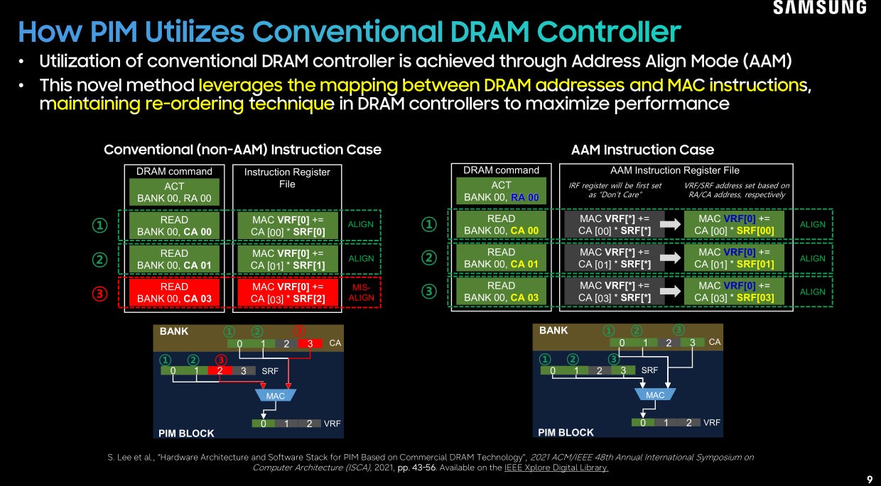
Enabling compatibility with existing DRAM controllers is huge. This trick is cool and seemed very painful to implement.
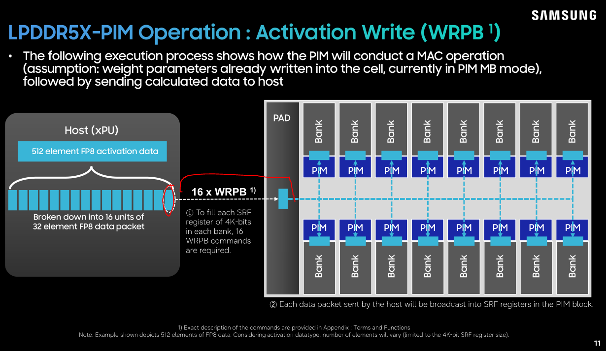
You can see the clever multi-cast system they made that is controler-compatable.
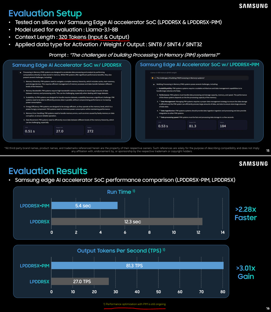
Two people in Q&A went after Samsung on the performance, implying it is quite underwhelming.
The presenter answered both questions with “we are still optimizing”.
Interesting but unfortunately useless engineering.
[2] Networking
Last year networking section was so much better. SAD!
[2.a] Broadcom Thor Ultra
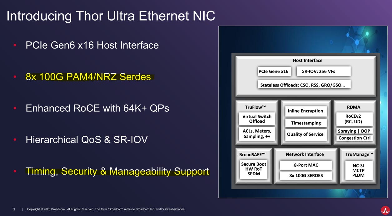
Someone in Q/A session asked about 200G SerDes version. Presenter said it’s on the way. Not that difficult to plop in a new PHY for 4x200G.
To move this to 8x200G, the entire chips digital logic would need to become significantly larger and timing closure would be more difficult but nothing crazy.
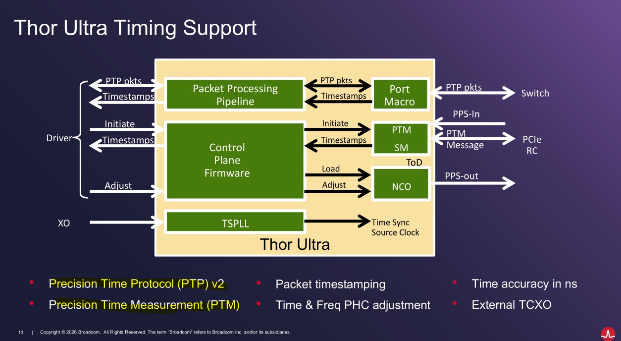
Timing/sync support discussed by Meta at OCP is included. Very cool stuff go check it out here.
OCP Global Summit 2025: Irrational Recap

Irrational Analysis is heavily invested in the semiconductor industry.
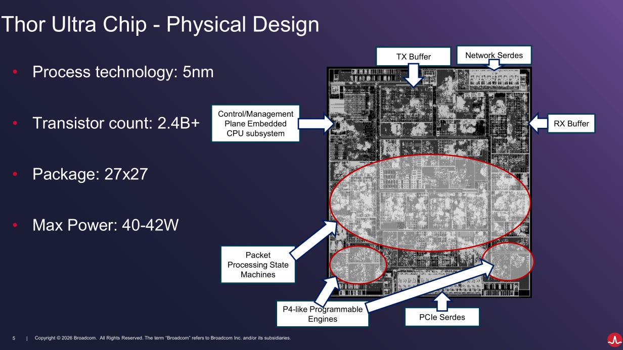
Thanks for the hi-res image. Let’s zoom in for fun on the analog bits.
Nevermind resolution is kinda bad. Can only spot the global PLL. Was hoping to label major inductors.
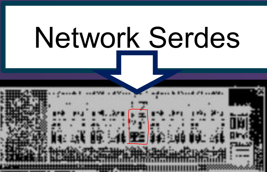
And the rest of this presentation is boring upper layer packet stuff. Moving on.
[2.b] Nvidia BlueField-4: The Neocould NIC
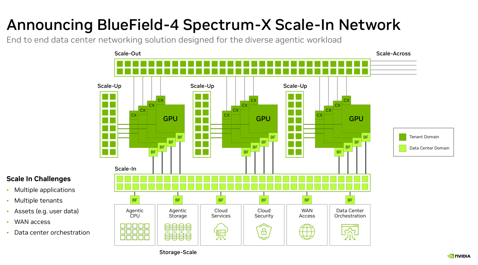
Nvidia is re-naming front-end as scale-in while Lumentum/Hurlston are using scale-in for something very different that is super not happening anytime soon.

Anyway, all you need to know is Nvidia BlueField DPU/NICs are comically overpriced and generally only used by Neoclouds.
Almost all the hypers have their own custom front-end NIC.
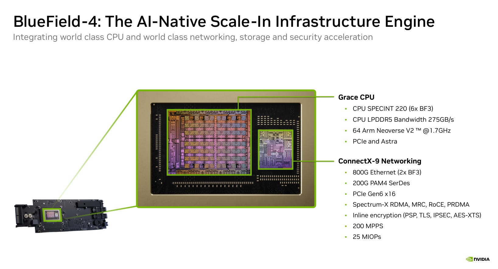
Nvidia Grace is legendary in a hilarious way. Will circle back to this in the CPU section. I have a conspiracy theory that Nvidia has excess Grace dice in storage and chose to slap it into this NIC.
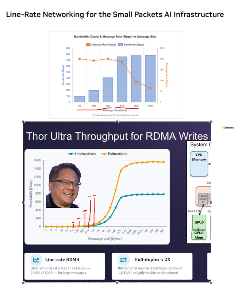
Nvidia BlueField 4 crushes Broadcom Thor Ultra in small package size tput.
[2.c] Nvidia Spectrum-X Multiplane
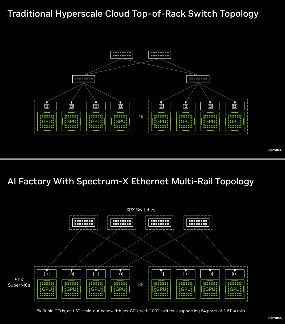
The Nvidia presenter spent a good 5 minutes explaining why multi-rail is better than traditional tree. Microsoft idiots might have accidentally learned something here. More on that later lol.
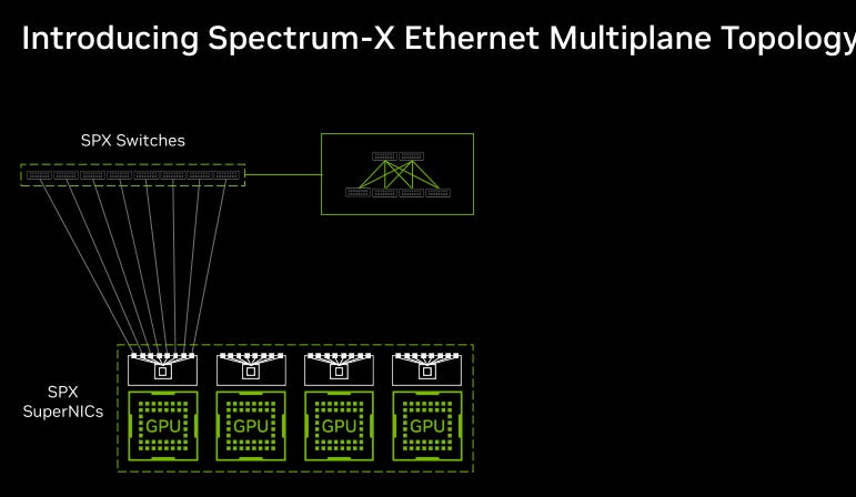
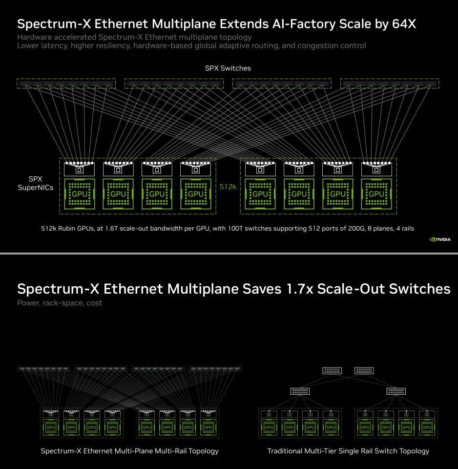
The key to understanding what is going on is this part of the diagram.
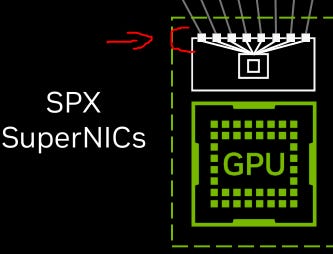
Each of the white squares represents a single SerDes lane of 200G in the 8x200G = 1.6T Ethernet port. They are mapping each lane of the NIC to a different switch. Curious how the physical wiring of this setup works. Probably some weird squid-like MPO connectors.
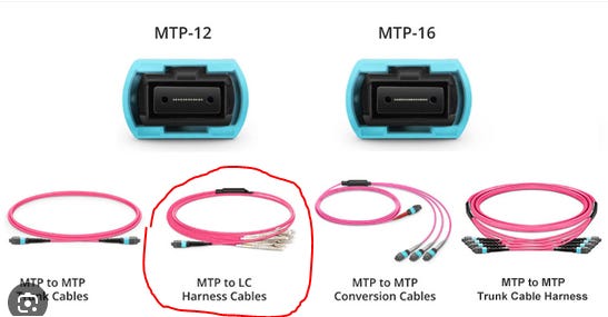
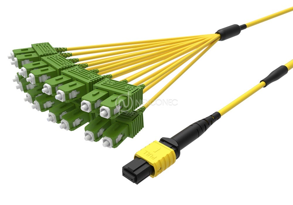
Probably something like this. Does not have to be LC on the other end there are other options. Lose maybe 0.2-0.4 dB in additional loss from the extra connection points.
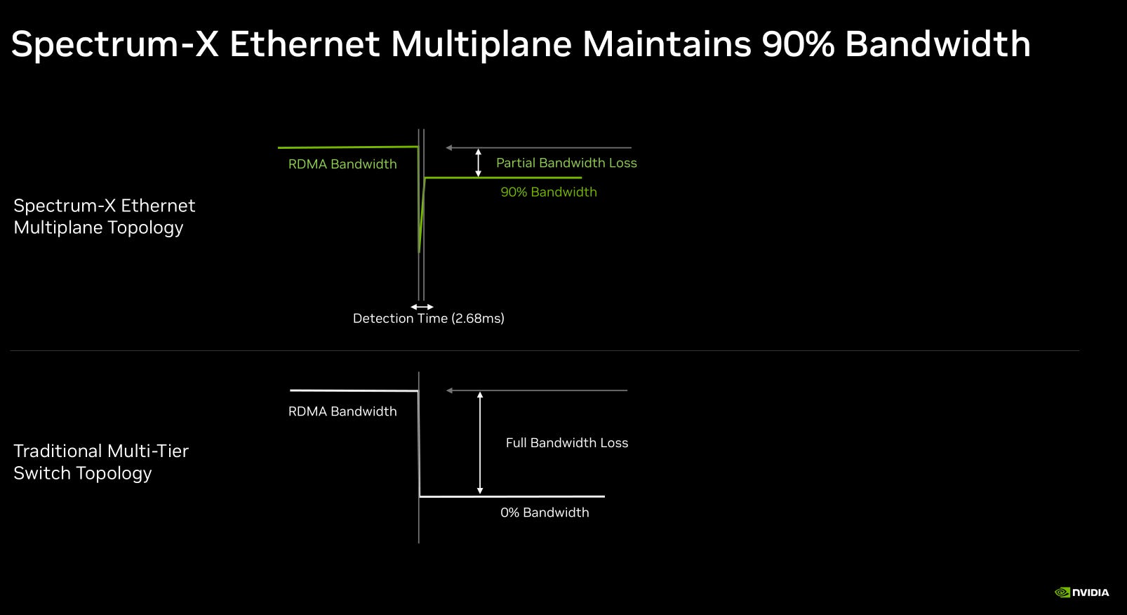
In a way, this multiplane trick also helps with redundancy. If one link flaps, there is a small bandwidth penalty instead of all the bandwidth go poof.
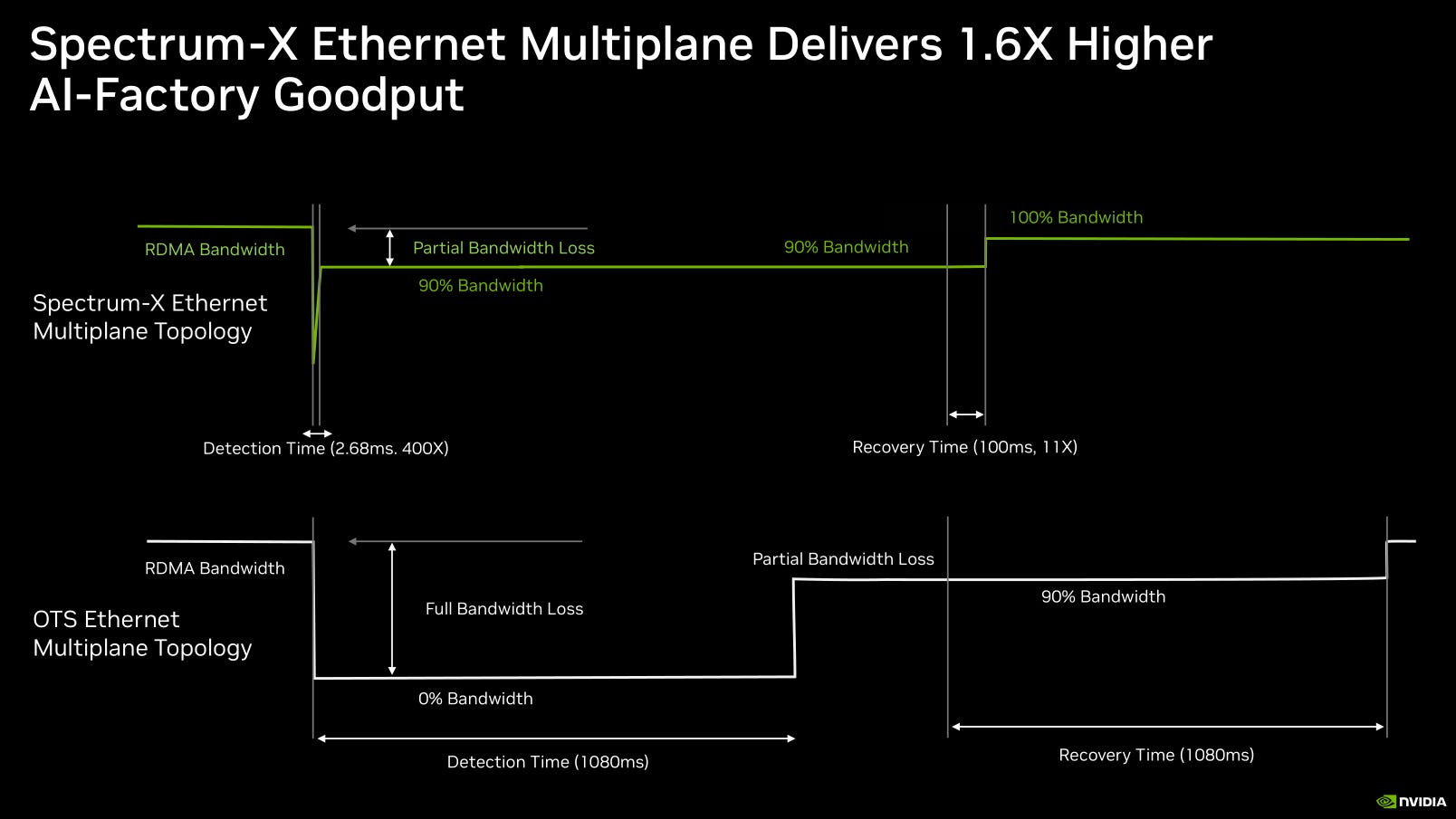
Very cool stuff.
[3] AI ASIC
Everyone has an ASIC, and yet Nvidia has half the CoWoS and most of the HBM bought up, at a discount too. Whoops.
The King Bleeds, Long Live The King

Irrational Analysis is heavily invested in the semiconductor industry.
[3.a] Meta: Worst of Both Worlds (Rec and GenAI)
Meta management forced their silicon group to optimize for recommendation and genAI networks. This is a fucking stupid decision but hey it means more revenue for Nvidia so good for my shares.
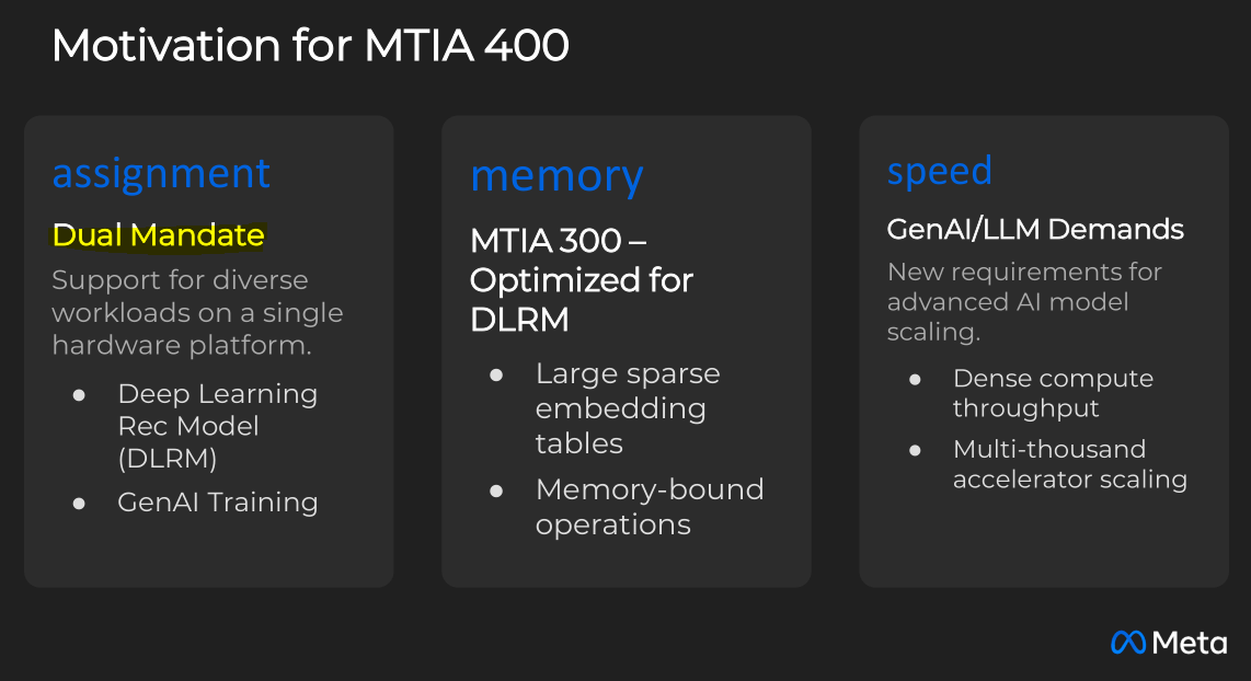
Zuckerberg has incinerated 10’s of billions of $ on metaverse crap but wont fund two ASIC teams for two very different workloads. WHY? This is remarkable stupidity.
Where the fuck is that picture one moment.

Sunscreen == accidental clown makup
Zuck == clown
I rest my case.
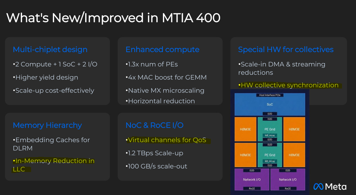
Highlighting the interesting features.
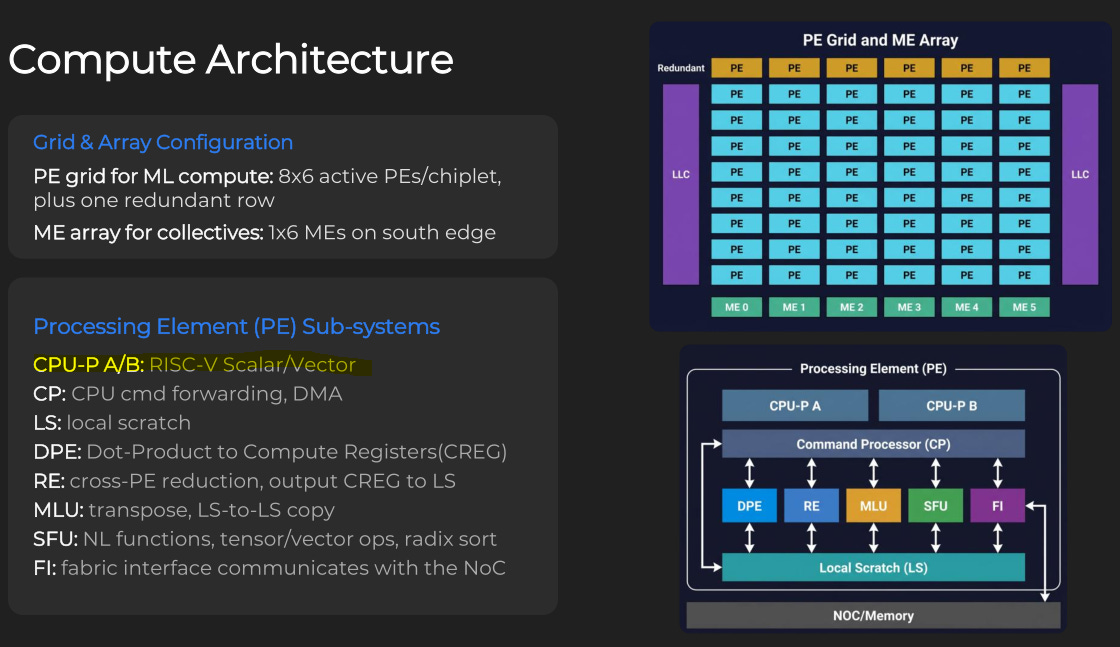
The RISC-V cores are tiny and for finite-state-machine and basic control. Similar to Tenstorrent “baby RSIC-V” architecture. Don’t get your hopes up RISC-V fans, you are still irrelevant in high-performance and (more importantly) user-facing scenarios.
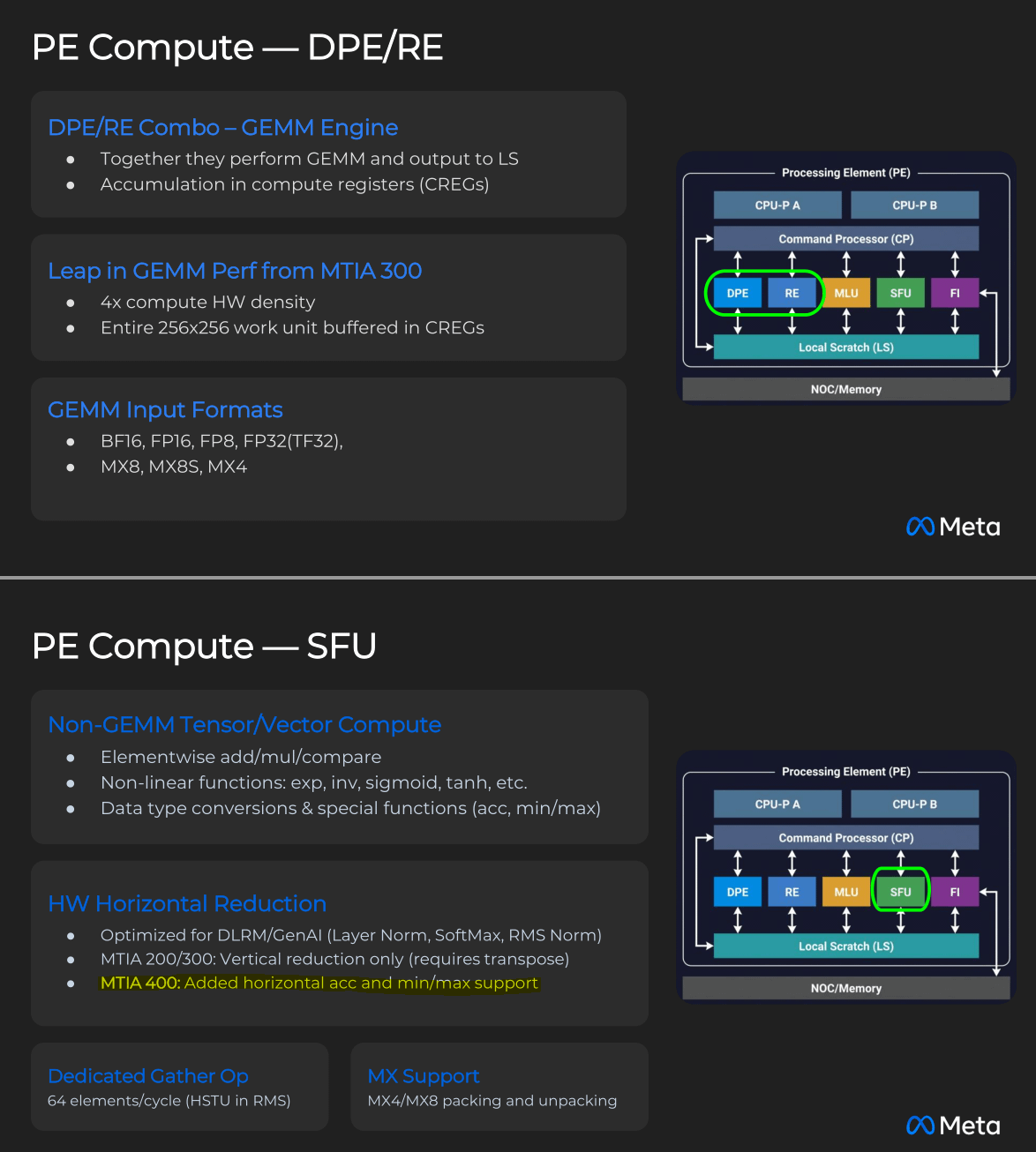
Avoiding the transpose is a nice trick. Curious on the implementation. Maybe extra paths on the internal PE routing network?
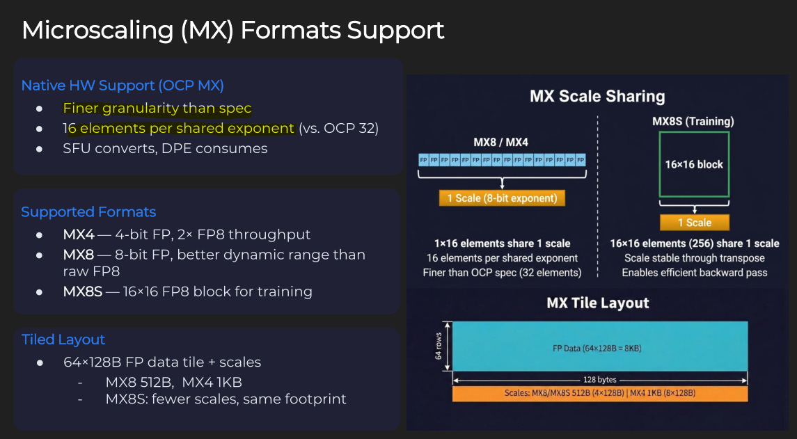
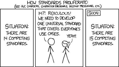
Meta runs OCP spec and they chose to not follow their own spec lmao.
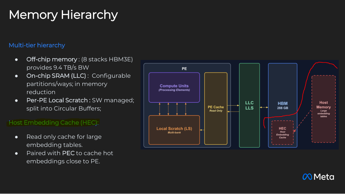
They dedicate some of the HBM for embedding cache. This hurts genAI performance unless there is a way to turn this off. The presenter talked as if this is a hardware-enabled feature which implies no they can’t turn this off. Great job with the dual mandate guys.
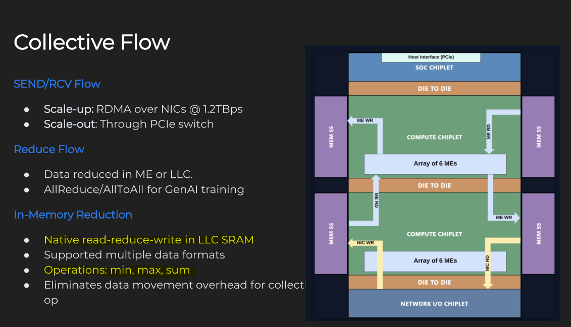
Neat feature. Small amount of compute right next to LLC (cache) SRAM to reduce data movement. Probably a small MUX tree. Has to be very small and fast to keep up with raw SRAM bandwidth. The basic-ness of the operations also implies simplicity in the in-memory reduction design.
[3.b] Nvidia/Groq Rubin/LPU Disagg
For an understanding of how Groq architecture actually works, see this old (classic) post.

I will skip all the basic architecture stuff here and only cover the rack-scale rapidly developed product. Credit to Jensen, he saw a problem (OpenAI + Cerebras deal), acted decisively, and Nvidia+Groq employees delivered a real product in less than a year. Set aside what you think about 144-wide VLIW architecture (I fucking hate it), the execution delivered by this team is incredible.
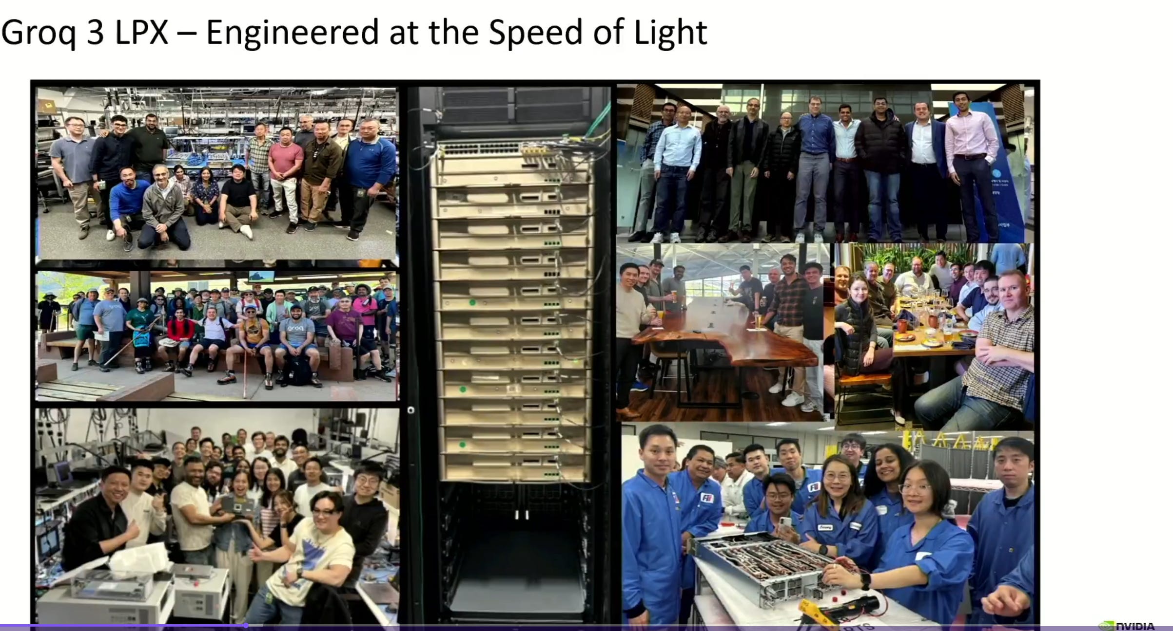
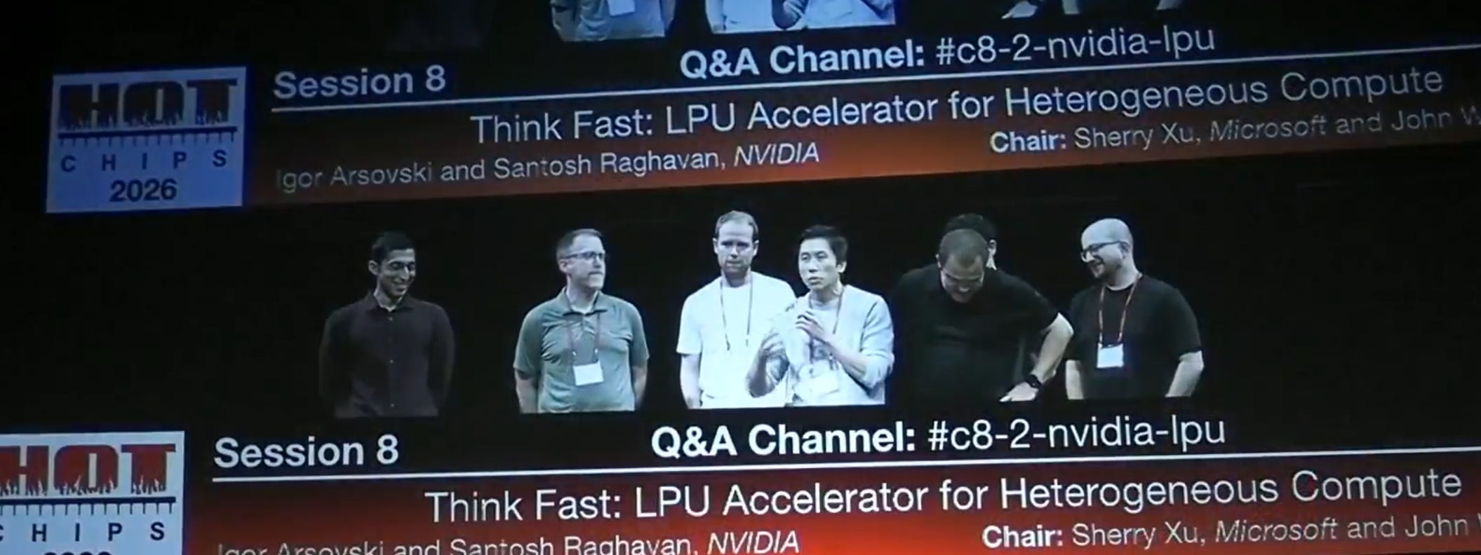
A bunch of them came on stage at the end and that was a nice moment.

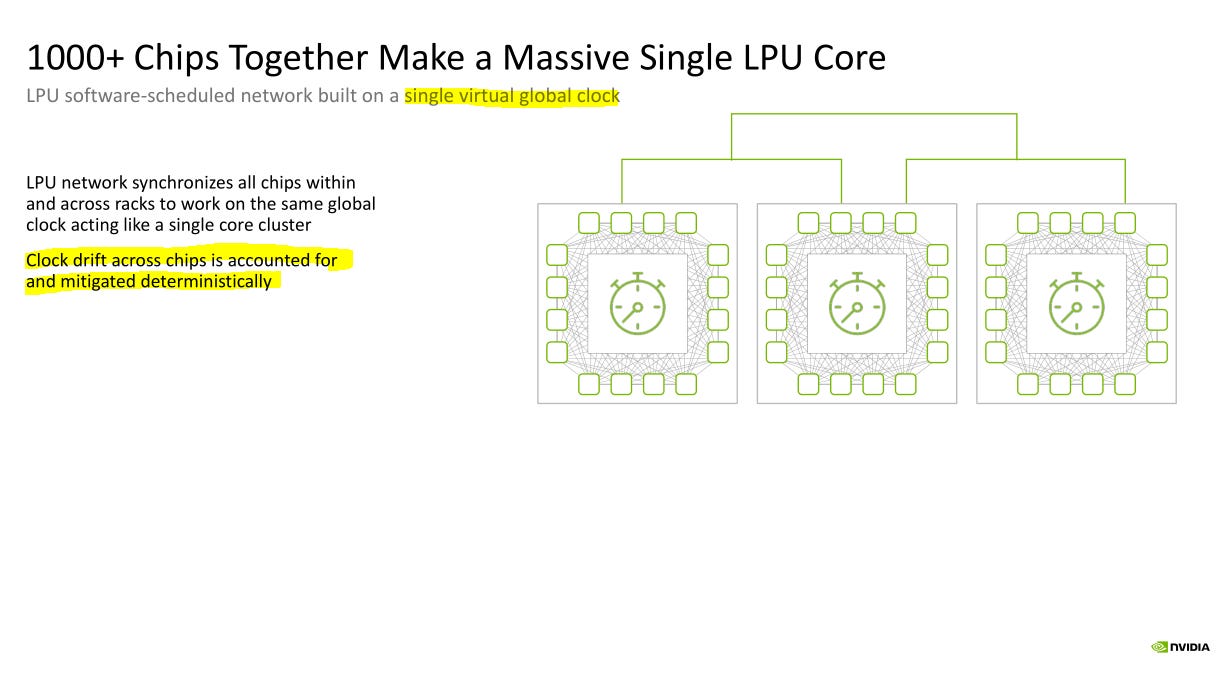
The way their “global” clock works is actually quite primitive. There are much better ways of making global, ultra-high-precision global clocks. Nvidia photonics group will help out with that. Quite curious how much improvement could come from an optical atomic clock.
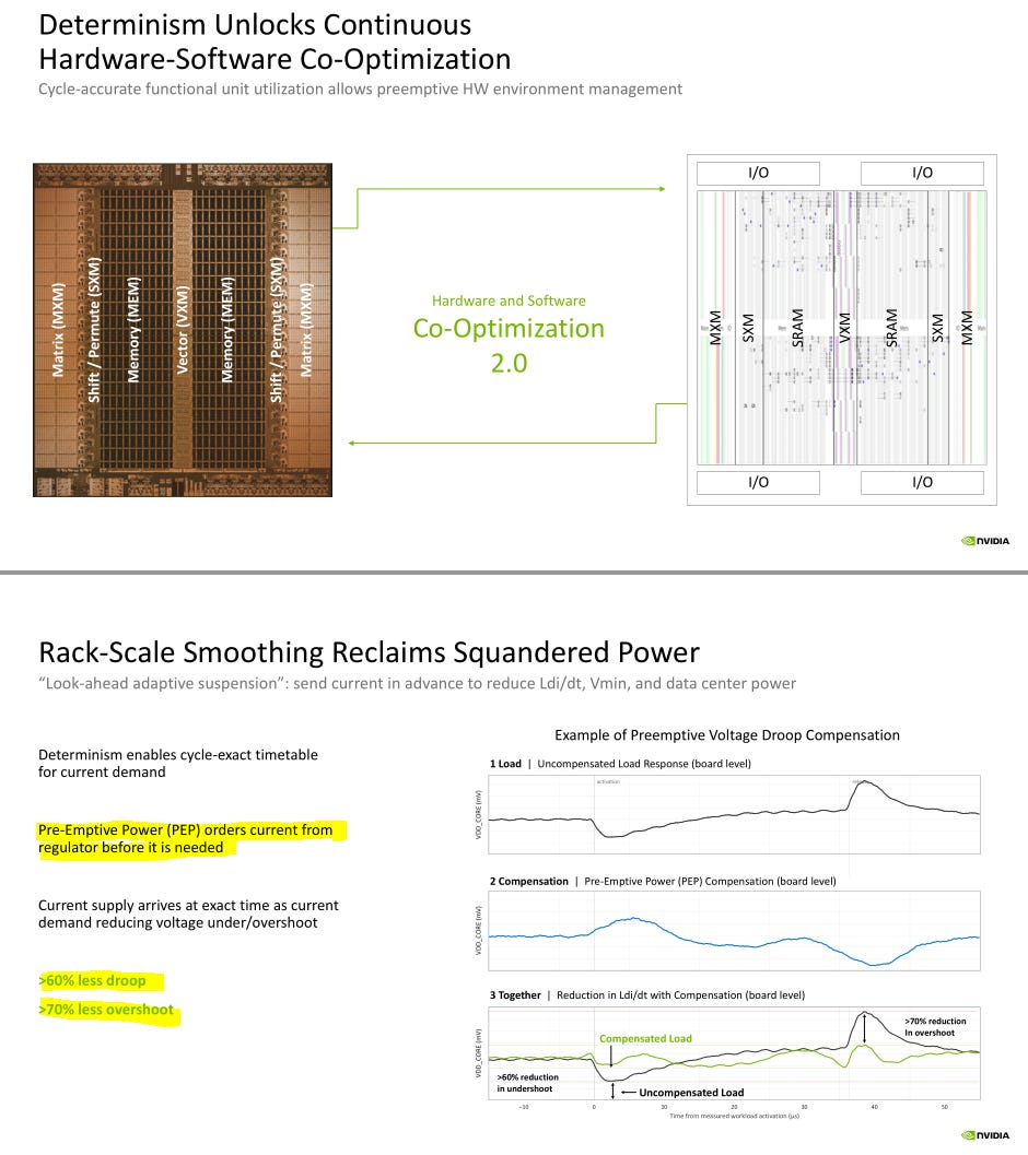
This is new and very cool. Could just use super-capacitors but I guess the Groq Haskel freaks saw an opportunity and executed well.
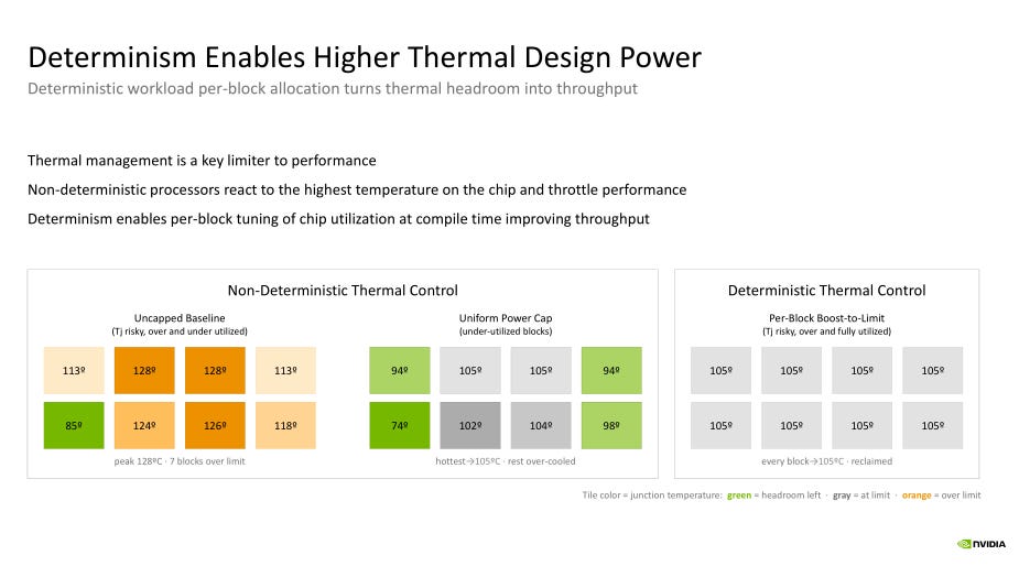
This part I don’t find believable. Variation in thermal contact pressure and process variation on the chip itself will make this strategy probably useless. Unless they spammed thermal sense diodes all over the chip in which case this is still useless because power monitoring and prediction (previous slide) accomplishes the same goal but better lol.
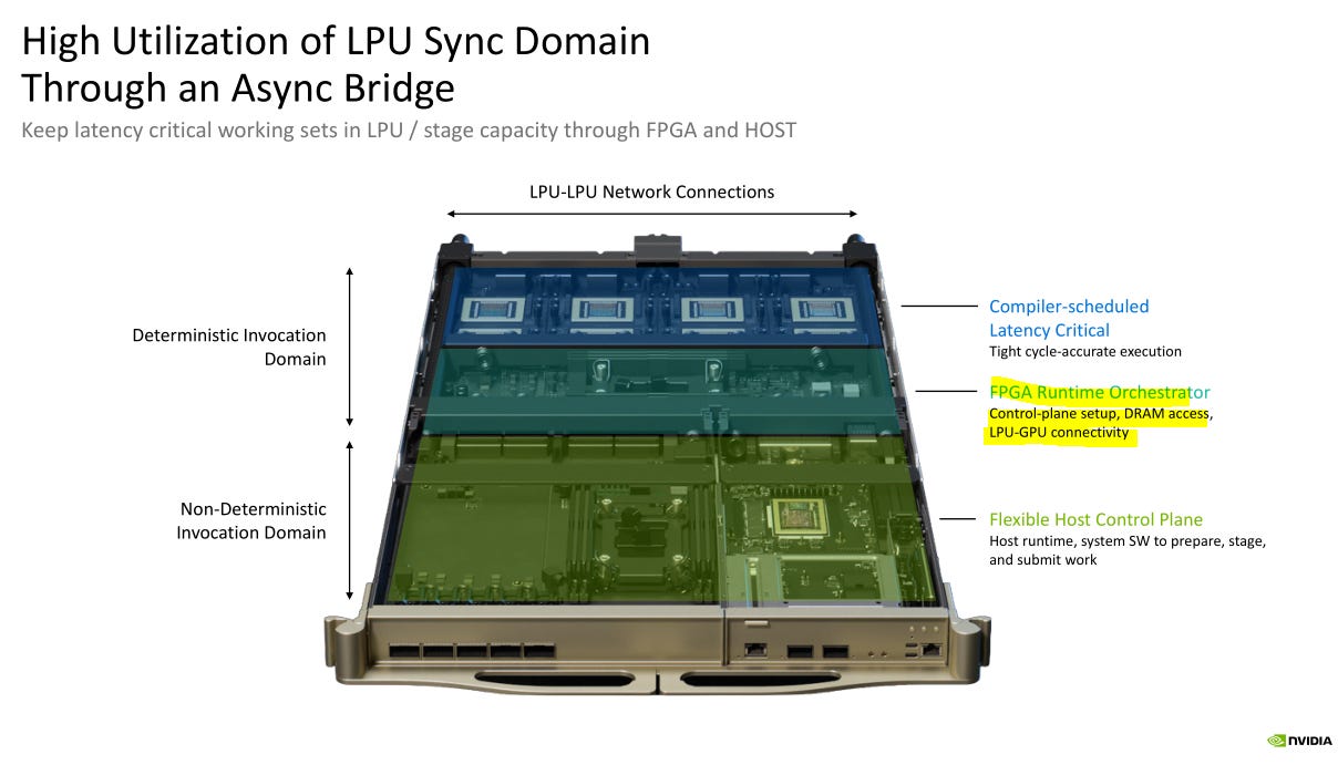
Next gen the FPGAs will be replaced with an ASIC. Probably minor gains (less power draw from control chips).
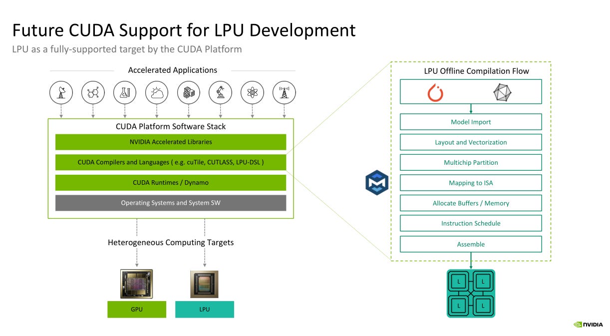
There is no chance this CUDA support happens and is any good. Go read my old VLIW post. This architecture is an abomination and the compiler is a hellish nightmare that must stay in hell. We cannot have a 144-wide VLIW compiler escaping into the world of normal software.
[3.c] Cerebras
Very little form the presentation is new compared to Supernova 2026 which was a week earlier. I did manage to talk to the presenter (JP) for 5-minutes and figured out a few things.
Cerebras Supernova 2026: Irrational Recap

Irrational Analysis is heavily invested in the semiconductor industry.
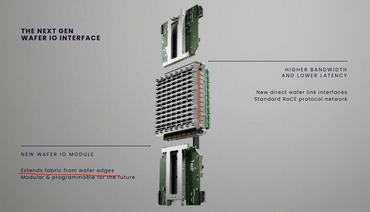
I asked JP about my conspiracy theory on the wafter I/O being a direct extension of the NoC. His response was to (poorly) pretend he did not understand my question which confirms my theory. This has implications for how they can scale the I/O going forward.
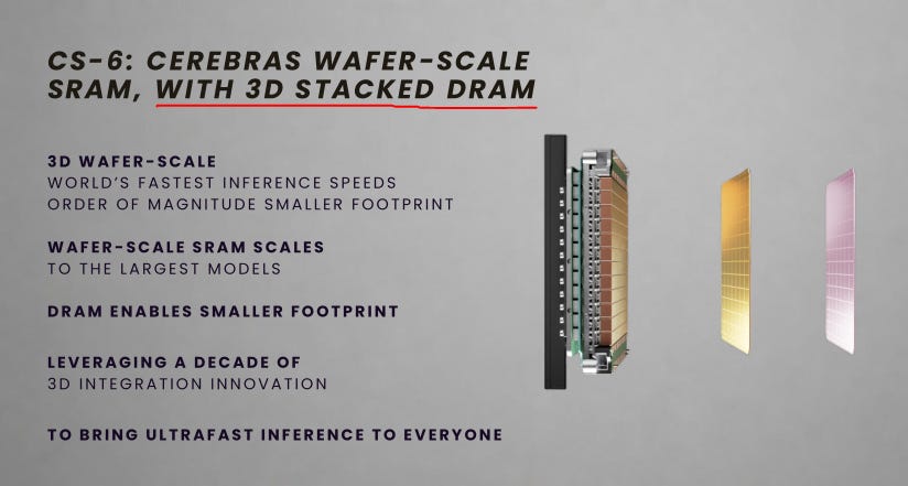
I think this is a mistake and 3D stacking a SRAM wafer is a better idea.
3D stacking SRAM (similar to AMD 3DvCache) leads to maybe an extra cycle of latency. No need to change compute access you simply have much more SRAM at 4-cycle latency instead of 3-cycle.
DRAM reliability at high temperatures is questionable. Same arguments I made in the D-matrix section apply here. Frankly much more severely apply.
Cerebras compute digital logic and NoC is not designed for DRAM accessing. D-Matrix had to make a huge amount of custom stuff just to get DRAM FLITs to work efficiently without a bulky traditional controller.
Historically, I/O is Cerebras greatest weakness. 3D DRAM integration is an I/O problem while 3D SRAM is far simpler in this regard.
If Cerebras (for whatever reason) insists that 3D stacking a DRAM wafer is better than a SRAM wafer, then they should acquire D-Matrix to help accelerate this effort.
Scroll back up to section [1.b] and re-read the D-Matrix section. Cerebras (really any 3D DRAM effort) has to solve many/all of the same problems D-Matrix already has.
There is real engineering synergy here!
Let’s briefly talk about disagg inference from a commercial perspective. A large portion of this section was cut and moved to [9.a] to improve flow.
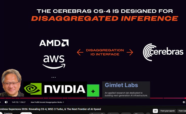
We were told that CS-4 is DESIGNED FOR DISAGGRAGATED INFERENCE.
And yet the most important prefill partner, Nvidia Blackwell, was omitted from the slides. It would be very embarrassing if a random startup (Gimlet Labs) got Cerebras+Blackwell disagg working way better and faster than Cerebras+MI450/Helios disagg.

These slides JP presented at Hot Chips 2026 really piss me off.
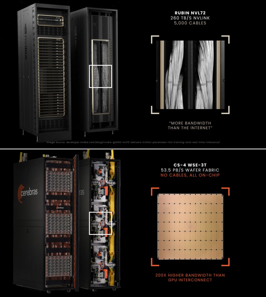
Dumbass, the AMD Helios rack is full of cables too. Arguably it has more cables because Nvidia removed internal flyover cables in Rubin. Trainium rack also full of cables.
YOU ARE ABOUT TO MAKE A HUGE AMOUNT OF MONEY FROM DISAGG WITH GPU SYSTEMS THAT HAVE A LOT OF CABLES. SHUT THE FUCK UP THIS DISHONEST STRAWMAN ARGUMENT. YOU ARE NOT TALKING TO BRAINDEAD VENTURE CAPITALISTS ANYMORE WHO LACK A SINGLE STRATEGIC THOUGHT IN THEIR SMOOTH BRAINS. PUBLIC MARKETS INSTITUTIONAL INVESTORS SEE THIS CLOWNISH BULLSHIT AND DO NOT LIKE IT.
In my 5-minute conversation with JP, managed to get enough information to confirm my parametric yield theory. He also said something so ridiculously arrogant I am not gona repeat it lol.
We are going to have so much fun in October/November.
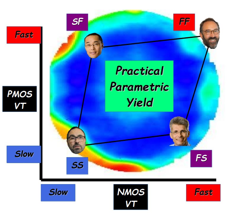
Large technical deep-dives take a long time. You can see the thumbnail for now.
[3.d] Microsoft Maia is still dogshit and embarrassing.
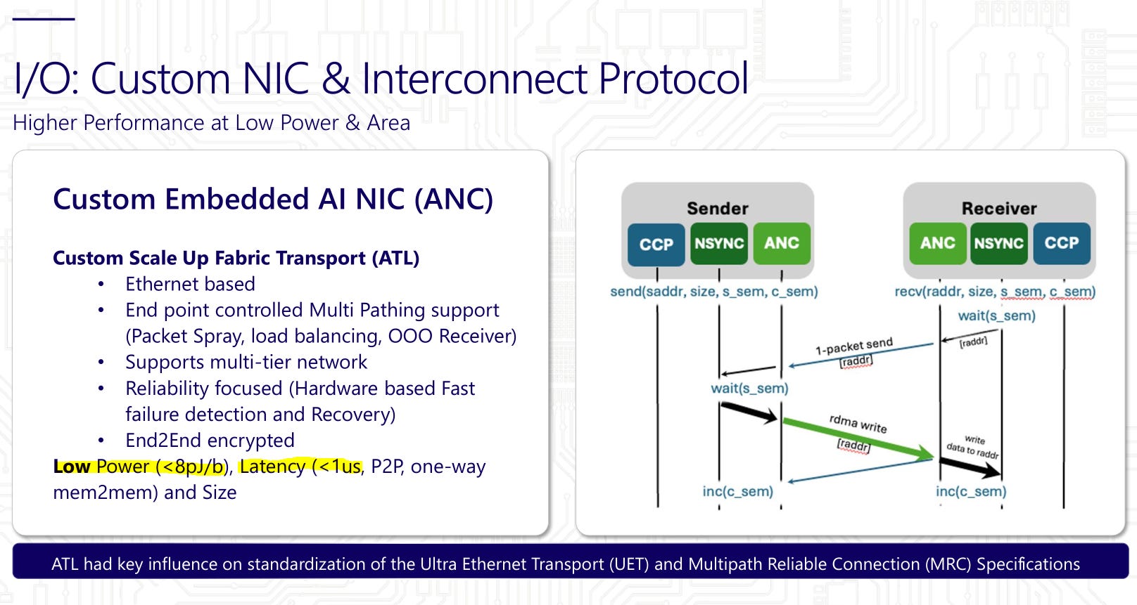
8 pj/bit is dogshit. So is 1 us latency. Especially when using 100G/lane class SerDes on TSMC N3P.
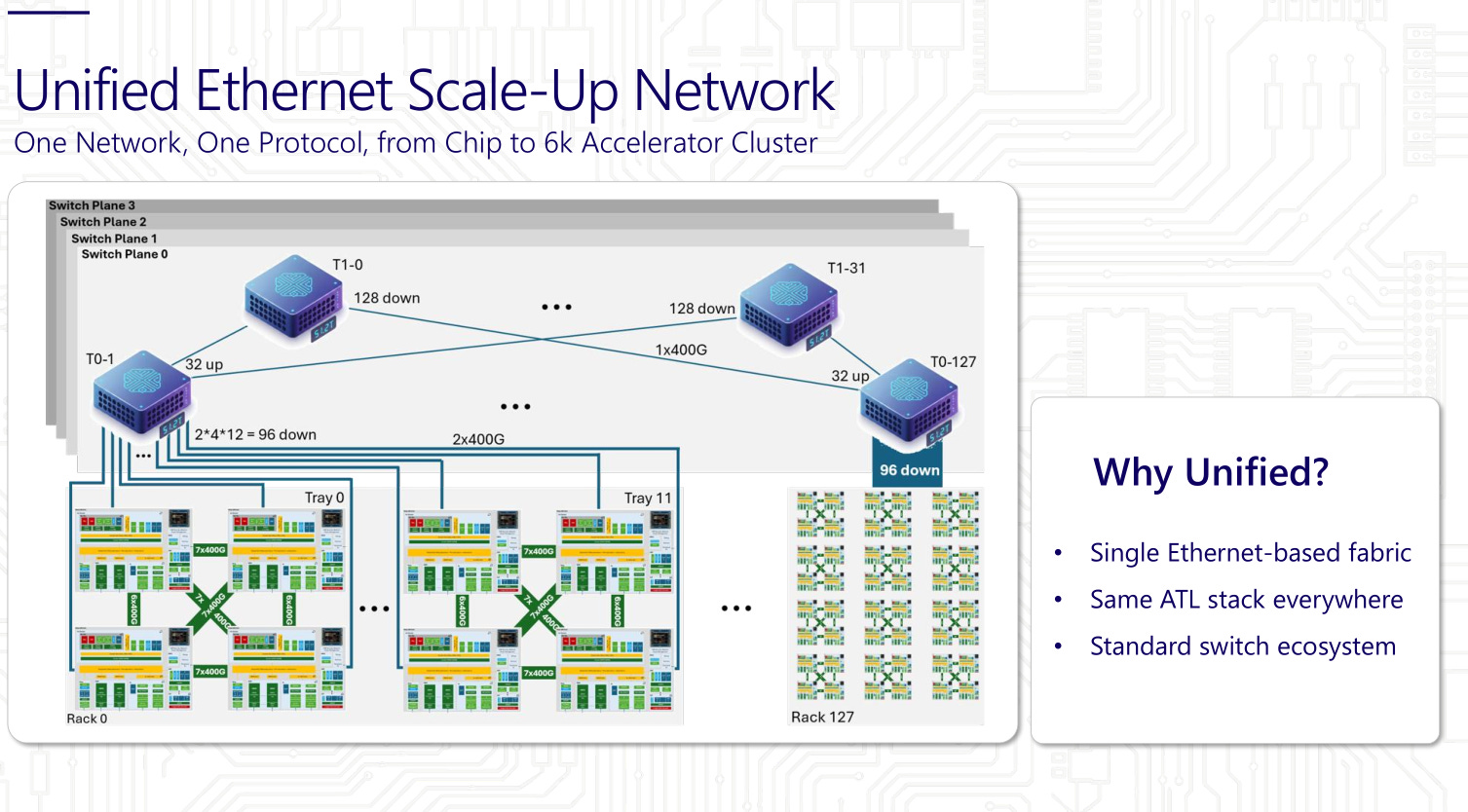
The Nvidia multiplane presenter literally spent 5-minutes explaining why this exact network topology is a bad idea.
If nothing else, maybe the Microsoft idiots accidentally learned something by attending Hot Chips this year.
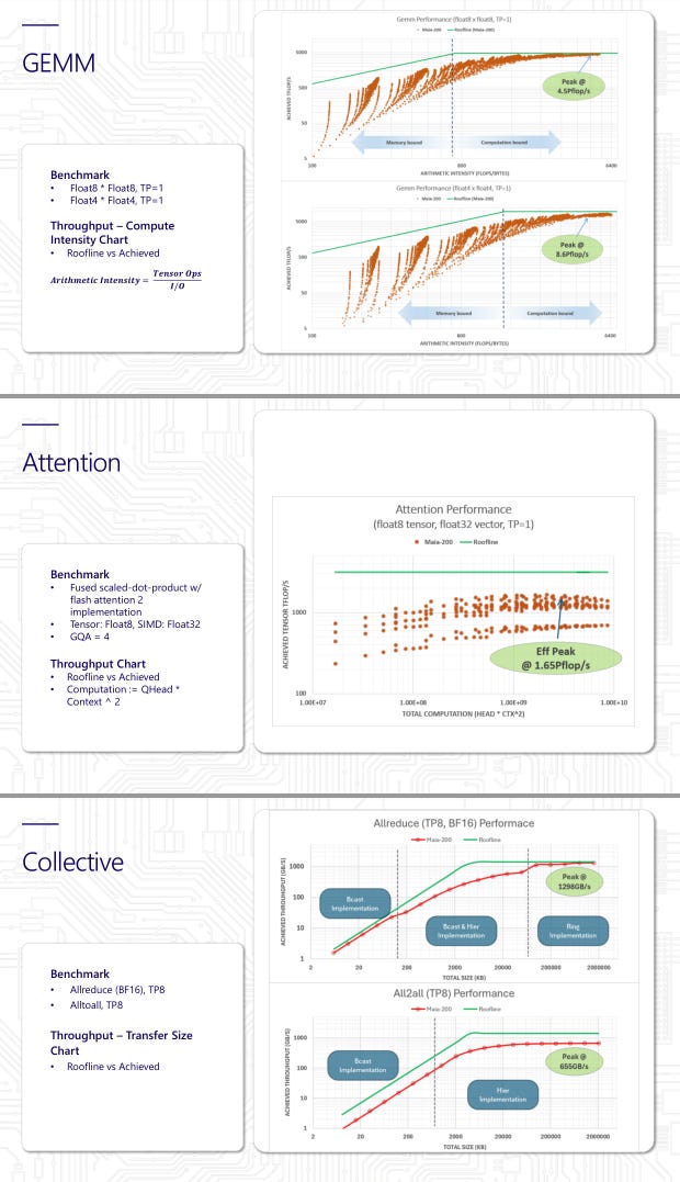
“Our chip is such dogshit we are too afraid to show benchmarks of it running real inference workloads so here are some lame micro-benchmarks that can’t be properly compared with anyone else.”
LOSERS
[3.e] Sambanova: Still Alive After Almost Euthanasia
Some countries allow doctor-assisted suicide for the terminally ill. A long time ago I watched a documentary on this.

The reason I bring this up is SambaNova almost allowed Dr. Lip-Bu to mercy kill them.

I like to imagine corporations as people. There is a failed presidential candidate who agrees.
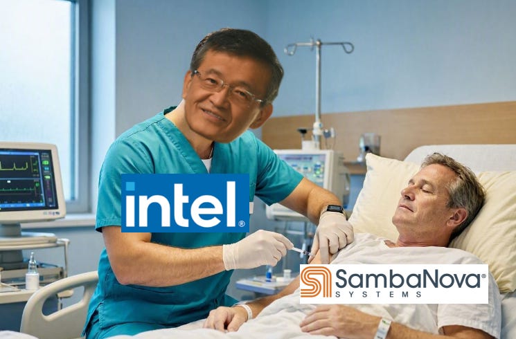
SambaNova was valued at $5B in 2021 and Dr. Lip-Bu was about to inject the lethal dose of anesthetic in December 2025 to put them out of their misery with a $1.6B deal that includes their debt.
But as the needle was going in, SambaNova saw the Nvidia/Groq deal on CNBC playing on the TV in the assisted-suicide hospital ward, ripped the syringe out of their arm, leapt out of bed, proudly screaming:
“I WANT TO LIVE!”
You have no idea how long I have been waiting to make this joke.

Ok joke intro over lets talk tech.
SambaNova is a CGRA. Think FPGA but more hardened and fancy.
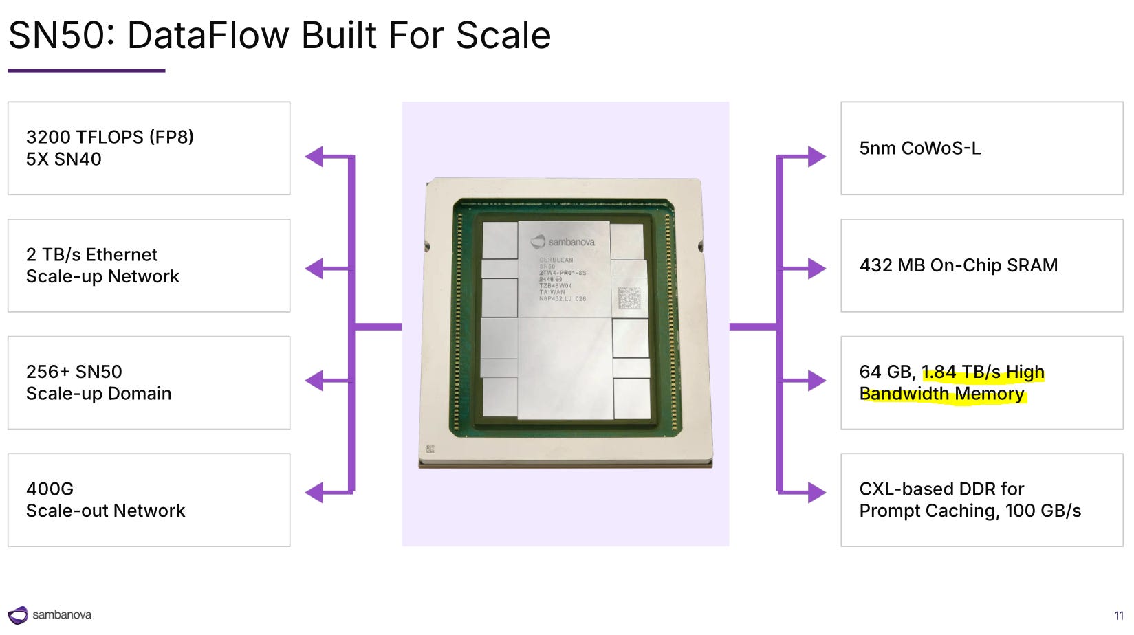
It’s HBM2e. There is a reason they did not include this important information. It’s because nobody makes HBM2e anymore and they are screwed on supply.
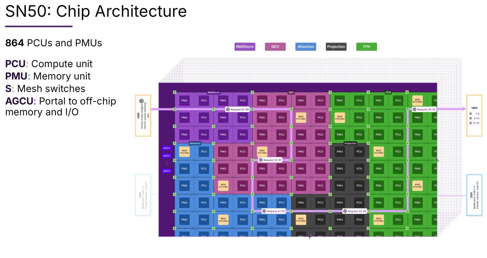
There is a degree of programmability like FPGA LUT logic, but much more hardened.
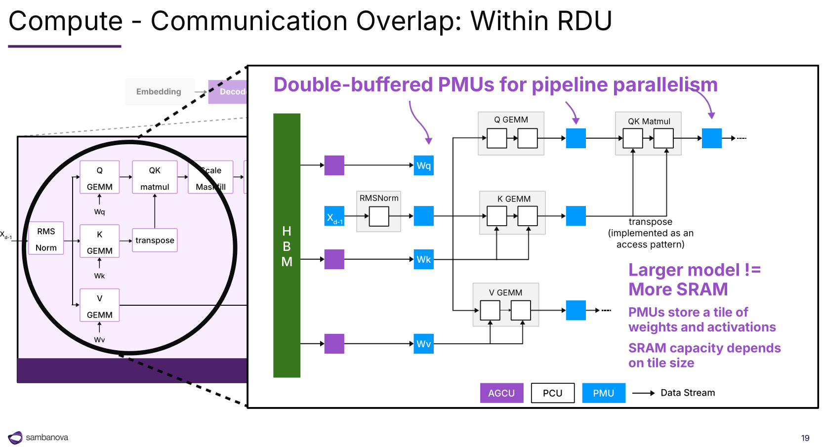
Parts of a model graph are mapped directly to hardware blocks. The coarse re-configurability allows for some communication overhead reduction.
Ask them what happens if input/output token ratio or context length changes. I’m sure this architecture does not have problems with dynamic inference workload changes. /s
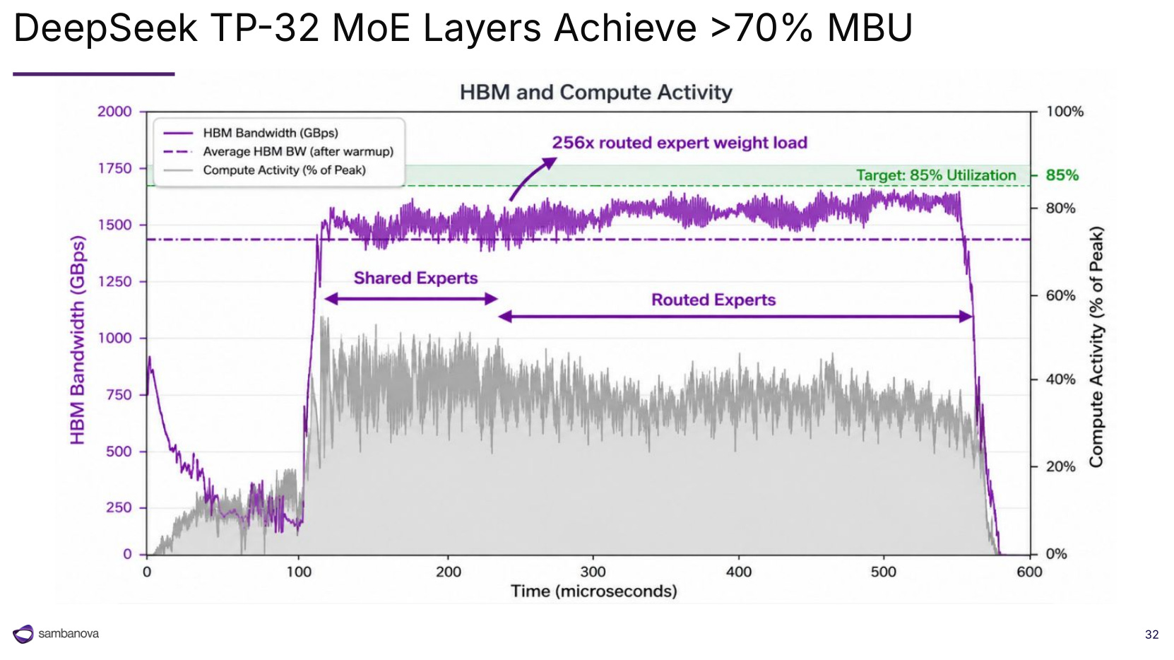
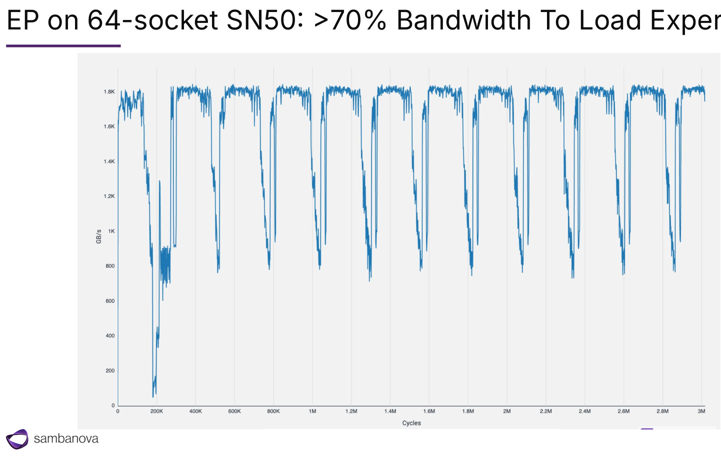
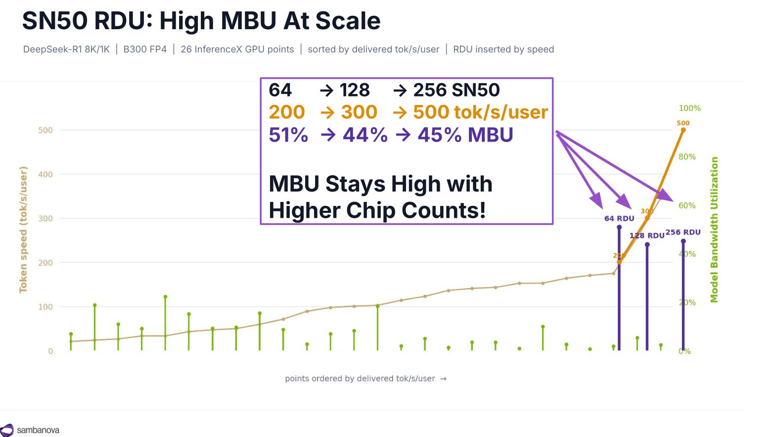
I know of a startup that is trying to achieve over 95% memory bandwidth utilization (MBU) consistently without using HBM or advanced packaging. Maybe I due-diligence all the AI ASIC startups and chose to join one of them for engineering dayjob.
[3.f] Google TPU V8
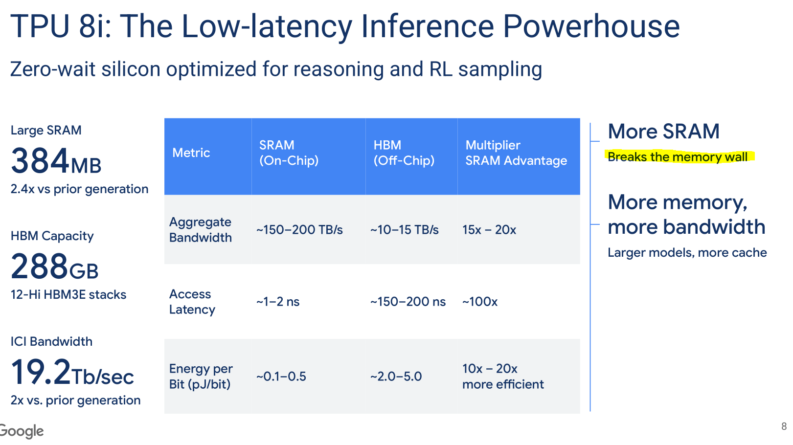
More SRAM breaks the memory wall? Really? Which marketing idiot wrote this? They should be fired.
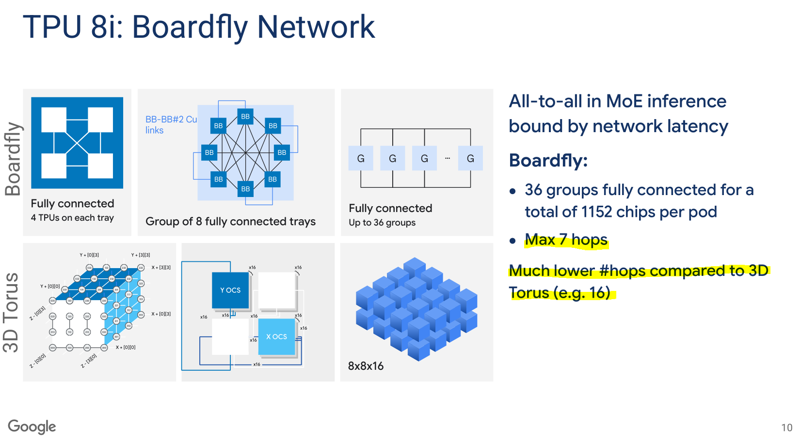
7 hops still not great. But this is real progress for MoE.
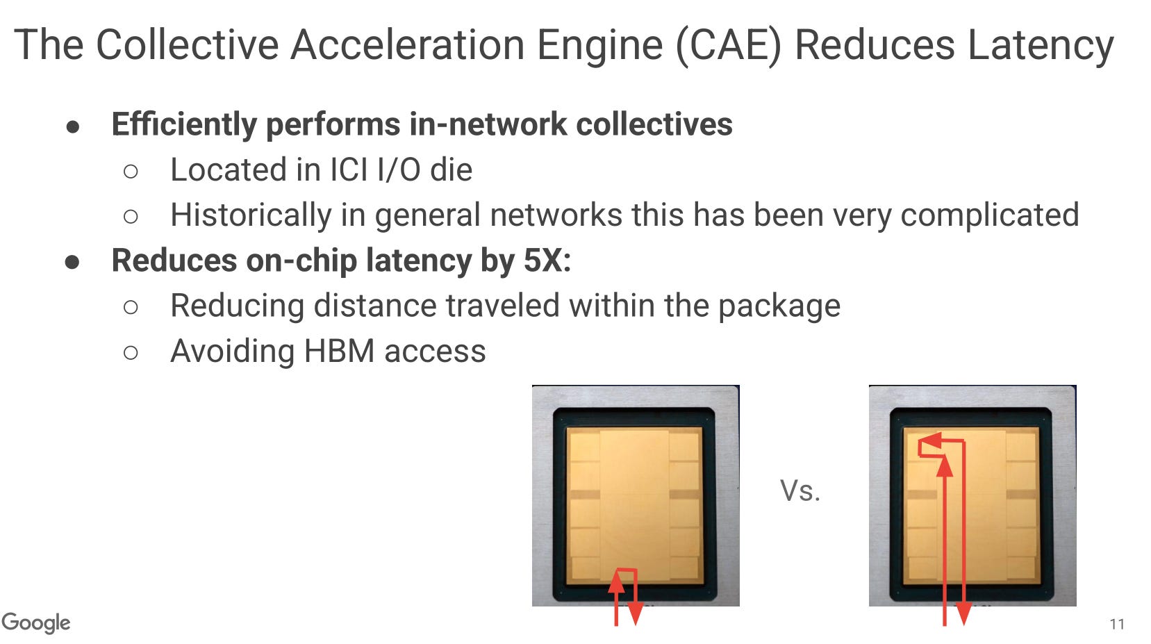
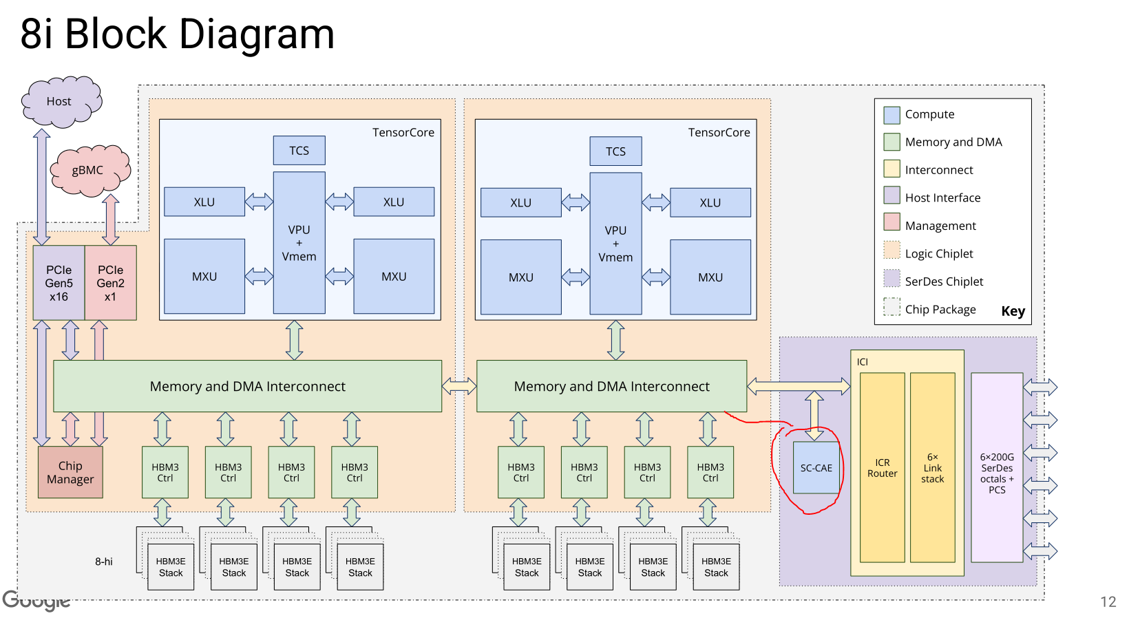
Interesting choice. Last gen this block (well similar functionality) was on the main die and sat on the crossbar. This seems like an obvious thing to do. I guess the tradeoff is significant die area. The collectives block probably has a rather large amount of SRAM to compensate for no easy crossbar access to HBM.
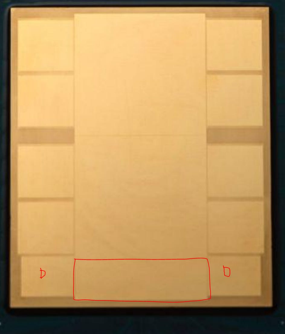
Easy to spot where the CAE+SerDes chiplet is. Sandwiched between two structural dummy dice. I have a good understanding of how large different type of SerDes are. This chiplet is maybe 20-30% too large to be just 48x lanes of 200G with some basic PCS and router. The extra missing area is the SC-CAE. Quite a lot of area.
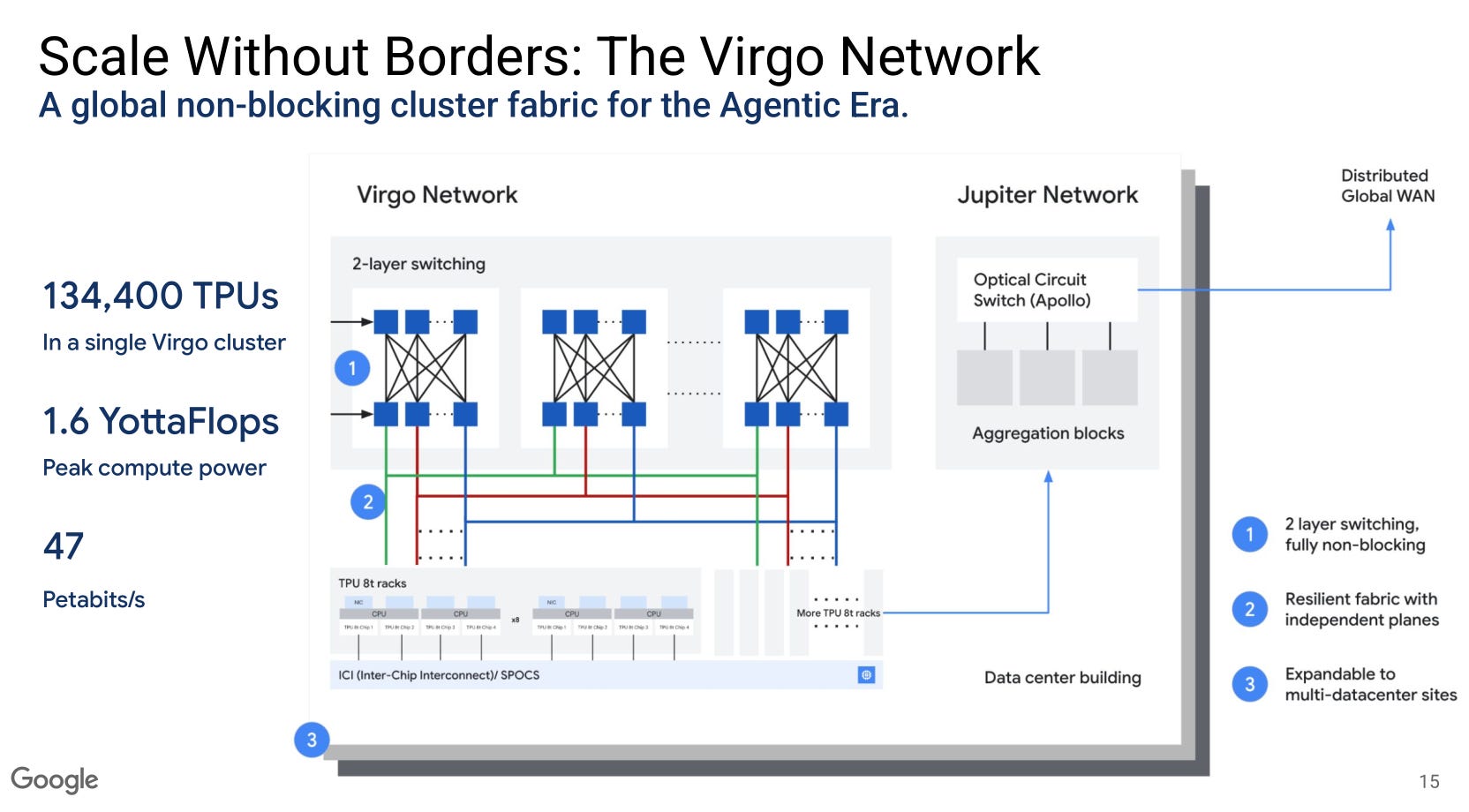
Two layer switching for the training cluster which is fine. Training is much more tolerant of latency.
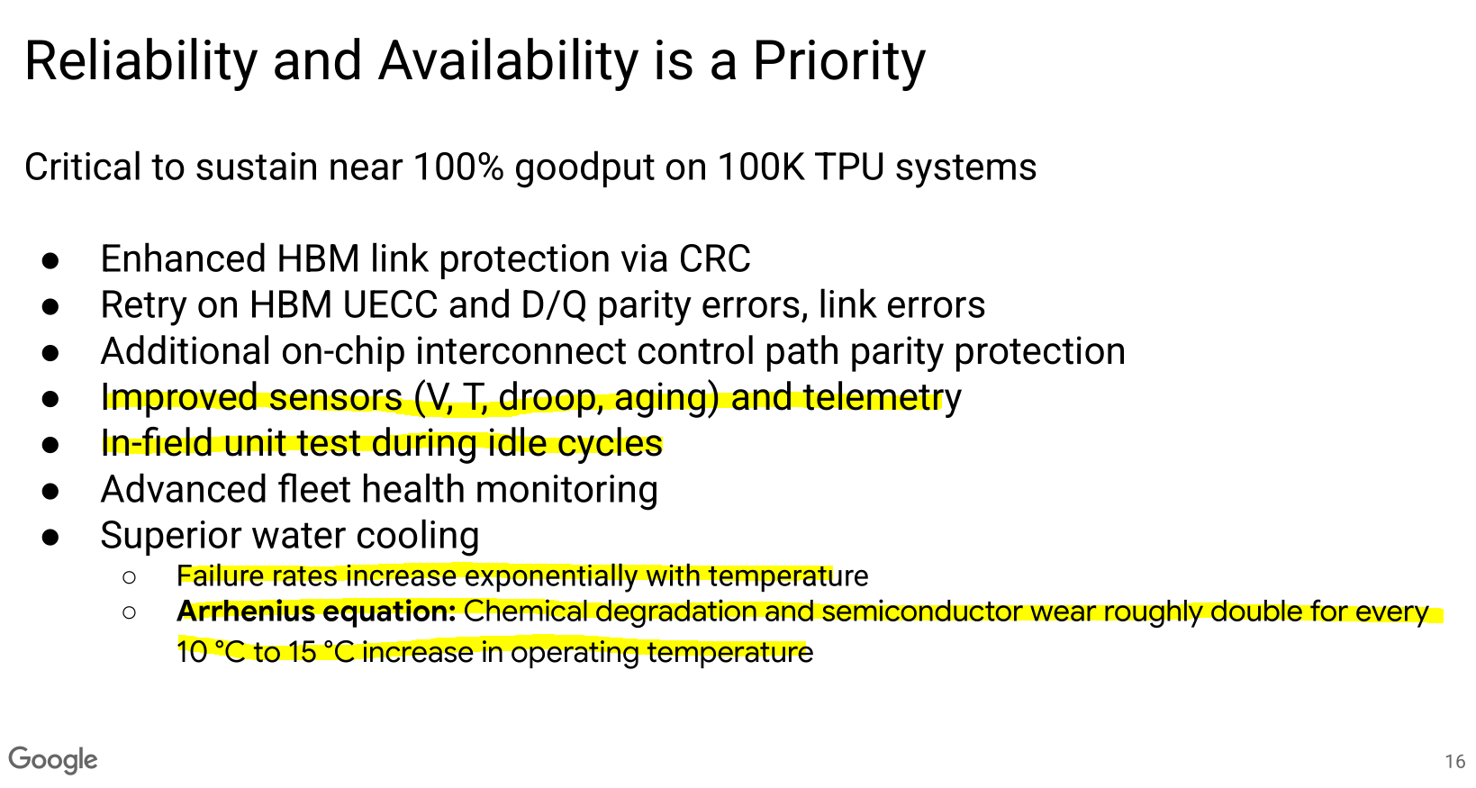
Hello HTOL my old friend. Putting more thought into on-die sensors is great.
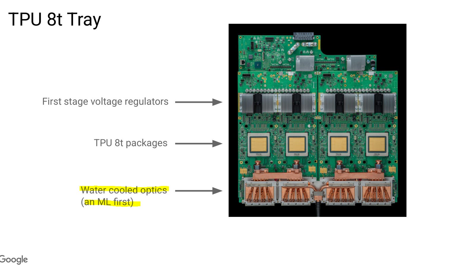
This is a trial run for NPO. Love to see it.
[3.g] OpenAI Jalapeno
Most of this section was cut and moved to sections [9.a] and [9.b] to improve flow. Will only cover small amount of stuff here.
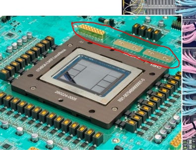
Those are Samtec Bullseye test connectors. Industry leading but a pain in the ass to work with. Mounting mechanism is tedious. Huber-Schuner MXPM is magnetic clip based but not good enough for 224G.
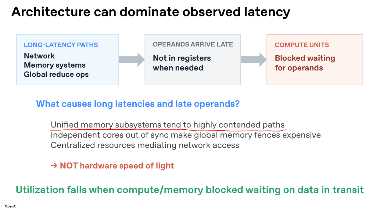
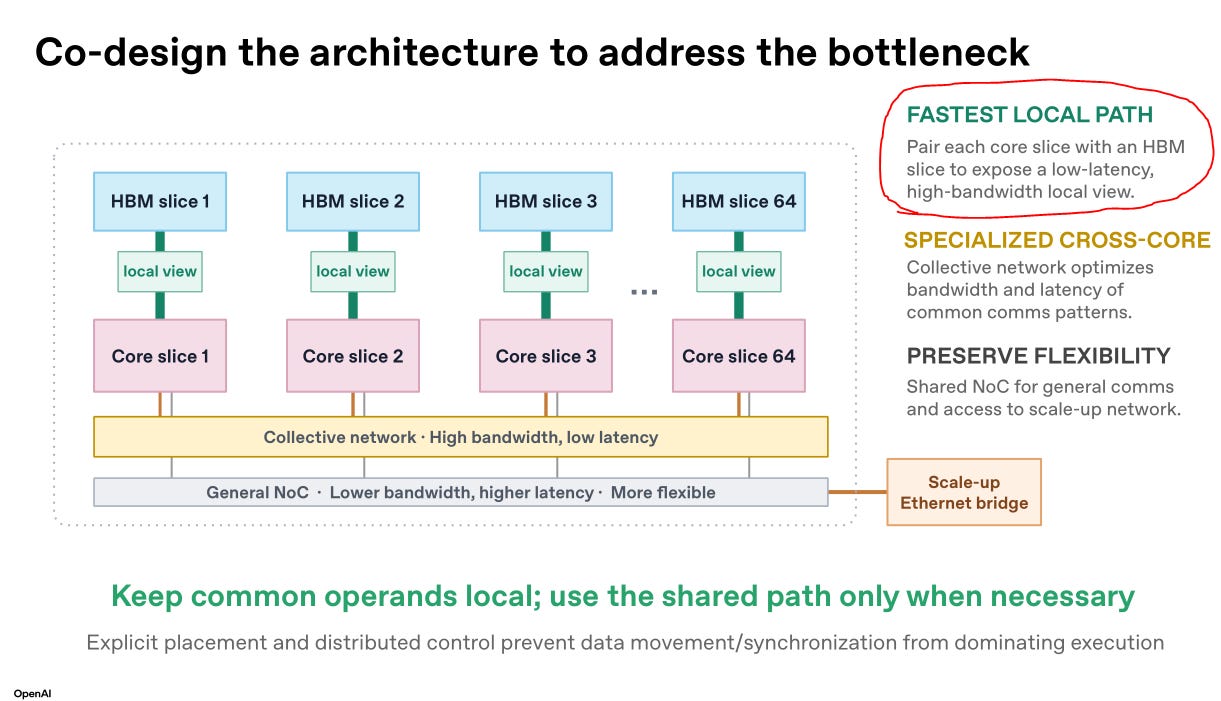
This is a classic argument. Historically, Intel CPUs have had private L3 per core while AMD CPUs have shared L3 across ~8/12/16 cores.
Other accelerators also use this. There are at least two entities I know of who do this HBM/DRAM/memory non-uniform NoC as a necessity, not a choice, but under NDA. Let’s just say there are tradeoffs.
Jalapeño also has out-of-order engines in the cores which is a very interesting design choice. To my knowledge, nobody has made this choice in AI accelerators so far.
CPUs have a variety of features that I like to call “black magic transistors”.
Out-of-order execution.
Branch prediction.
Speculative execution.
This blog I found years ago taught me the basics of CPU architecture and I hope you find it useful too.
https://www.lighterra.com/papers/modernmicroprocessors/
At a high-level, all you need to know is these CPU black magic transistors exist to speed up bad code automatically. Circuits that read assembly code blindly and somehow deliver huge performance gains, at the cost of massive power and area.
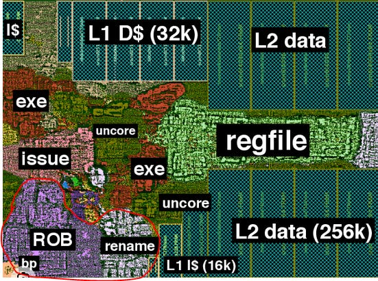
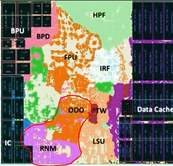
This is why these blocks don’t exist outside of CPUs, usually.
Bluntly, most of the Jalapeno presentation is actually quite boring. But this inclusion of OOO is fascinating.
Very interested in learning more about why they added this feature and how it is implemented. Size of the OOO rename buffer, latency, and so on. Send me an email.
[4] GPU
Very little new information so both the Nvidia and AMD presentations will be covered swiftly.
Only covering the Intel GPU to insult them. Raja Kodouri’s Xe architecture needs to be taken out back and shot. That entire group in Folsom should be fired. Intel can put their budget towards real things like fabs and CPU.
[4.a] Nvidia Rubin
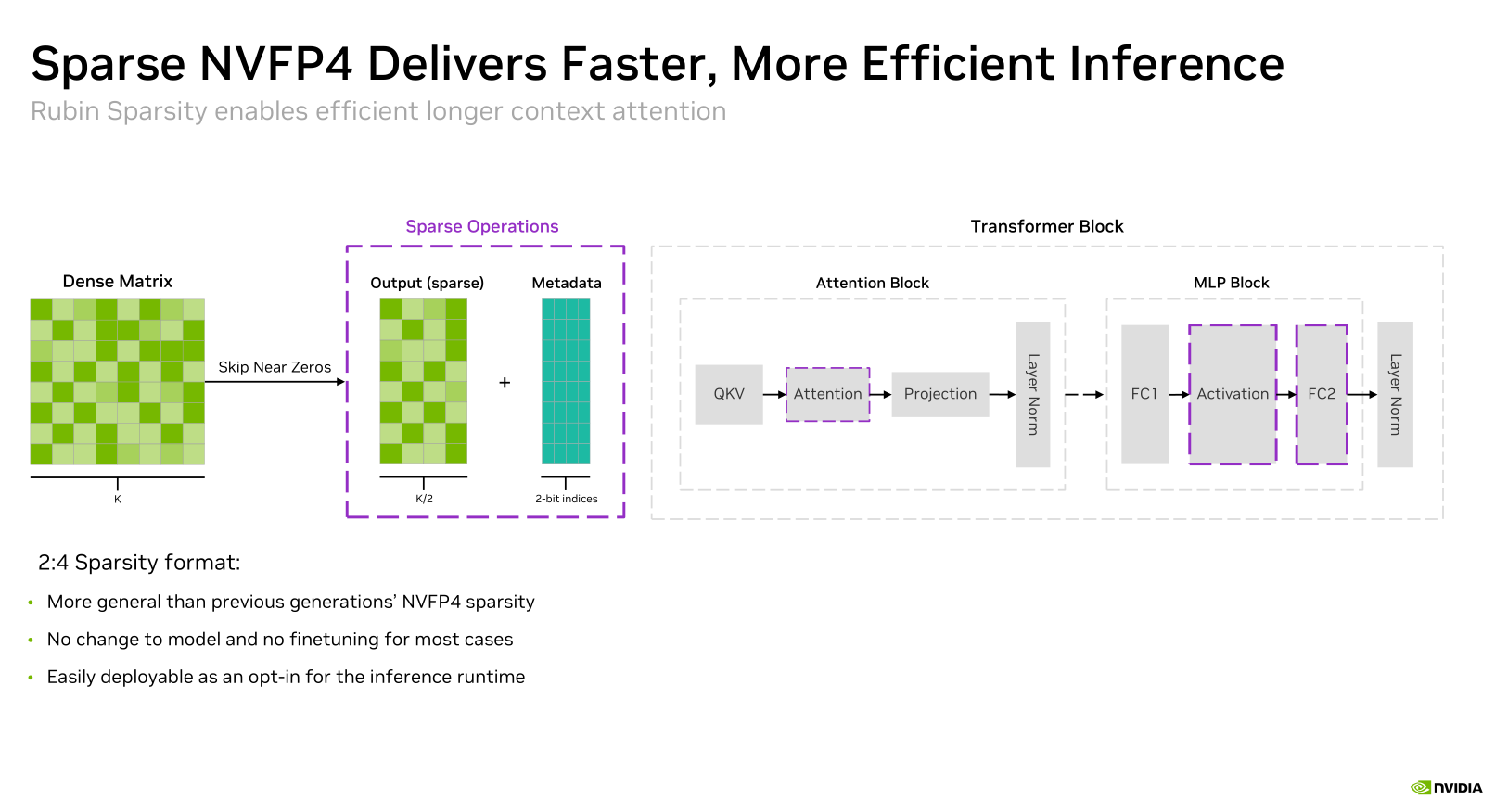
Weight sparsity is useless because expert sparsity is much better.
Here we have activation sparsity which is also probably useless. Nvidia and Cerebras keep trying to shove proprietary sparsity and it’s not going to work.
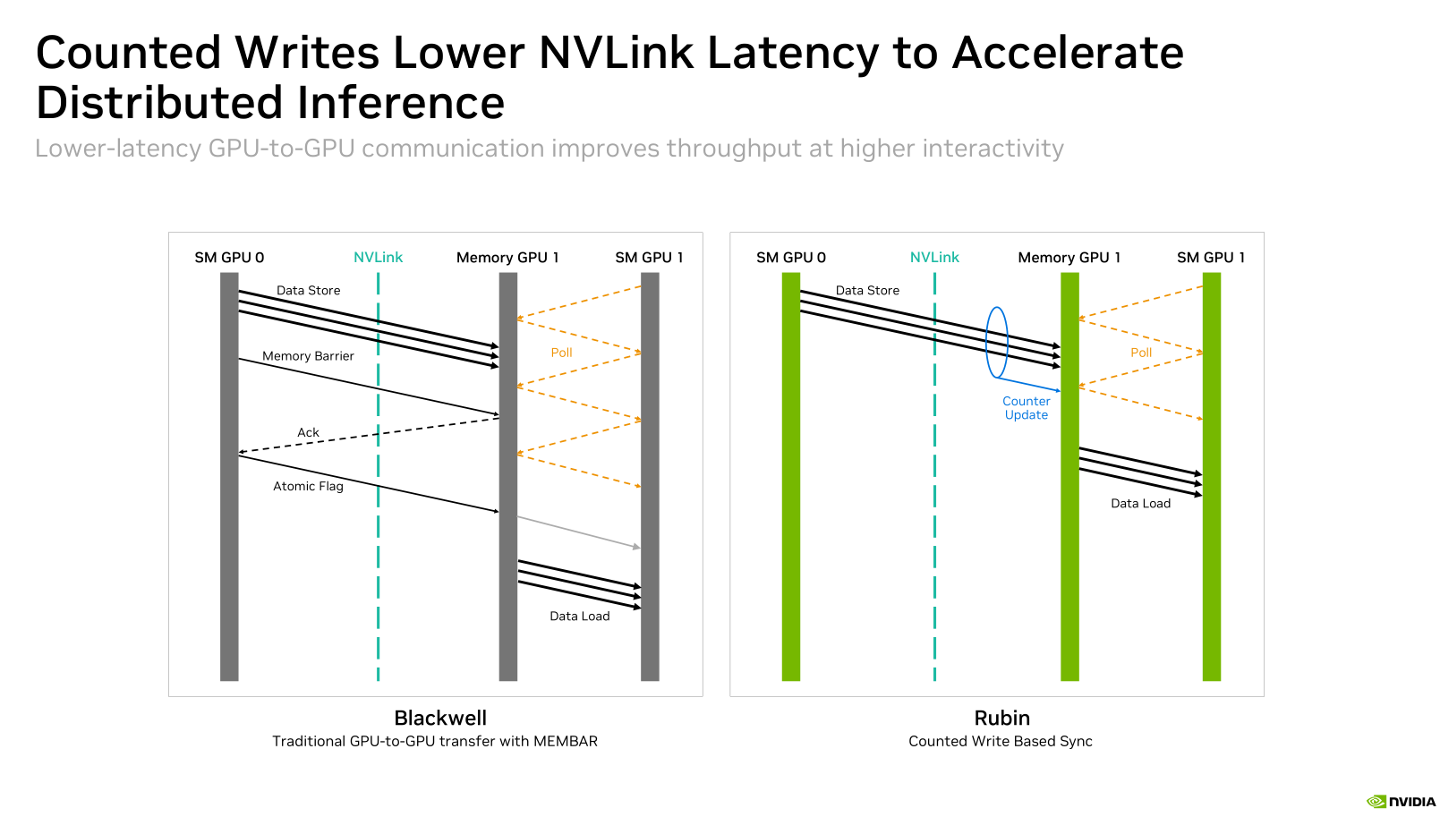
Embedding a counter into data packets. This is similar… what D-Matrix did with pinless DBI? Similar in spirit I know the context is very different. I suppose the penalty for this is the same. Some overhead and reduction in bandwidth.
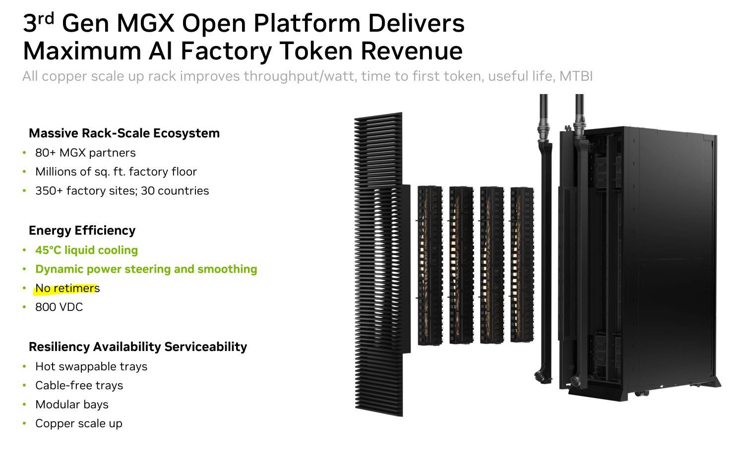
AMD’s rack is full for re-timers FYI.
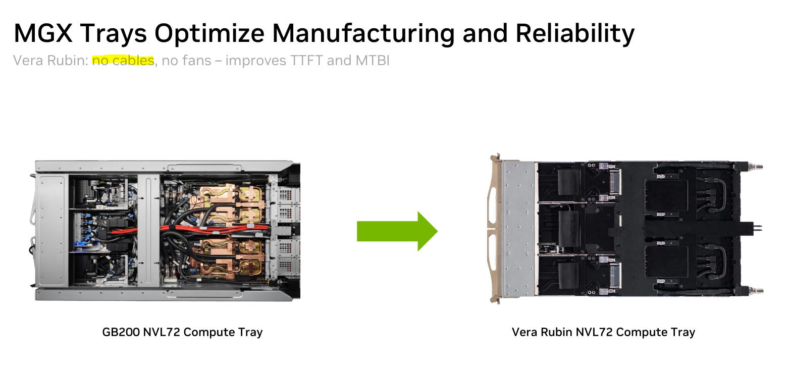
Cables have much lower loss than PCB but they get in the way of airflow. The connectors also are less reliable than mezzanine connectors on a PCB.
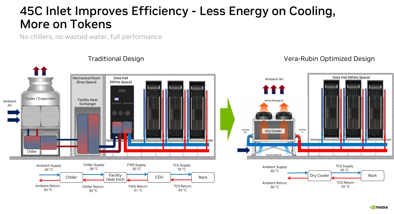
I propose we cover Antarctica in datacenters. We gona need cold ambient air for this to work. We can just deport all the penguins to the Middle East. Use penguin cuteness to bring peace to the Middle East.
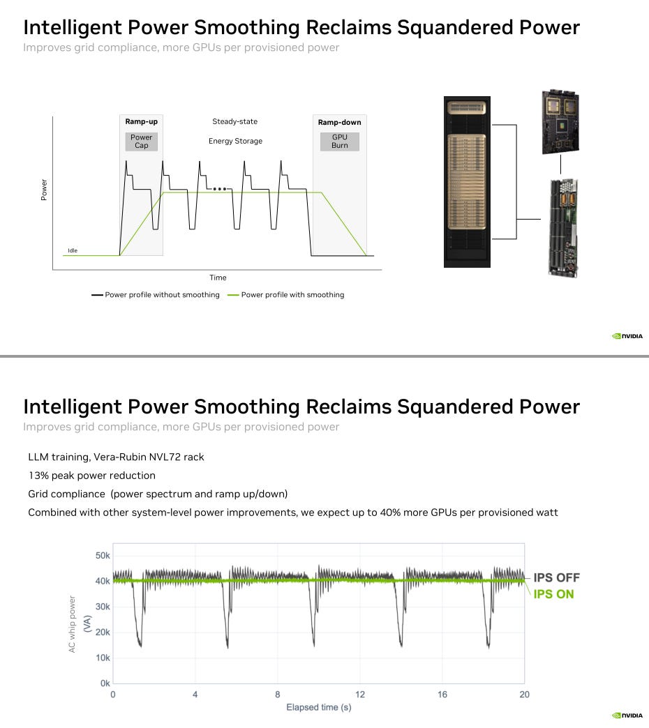
Annoying almost no technical details shared. Let’s zoom in.
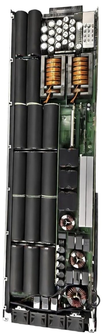
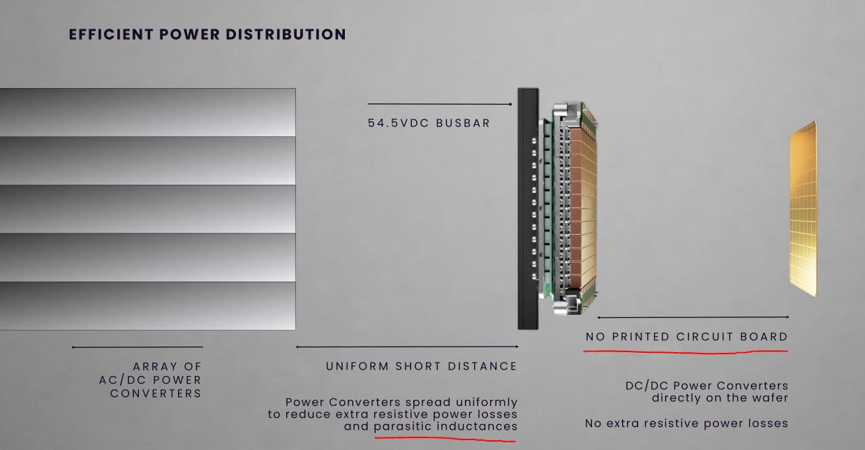
Ok it’s what I thought. A bunch of big capacitors and inductors. There are four fans in the bottom even though this board is full of passive components. Partially because even a small efficiency penalty leads to huge heat generation. Also because capacitor performance is very thermally dependent. Finally, capacitors tend to go kaboom when they fail. It’s very exciting.
[4.b] AMD MI400
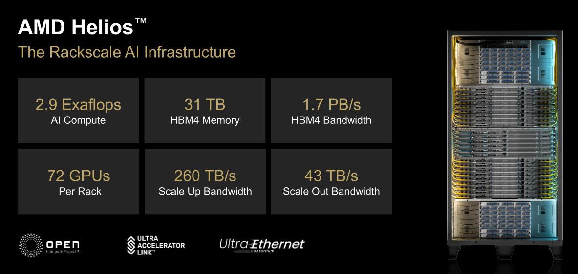
This rack is full of re-timers, harming TCO and latency.
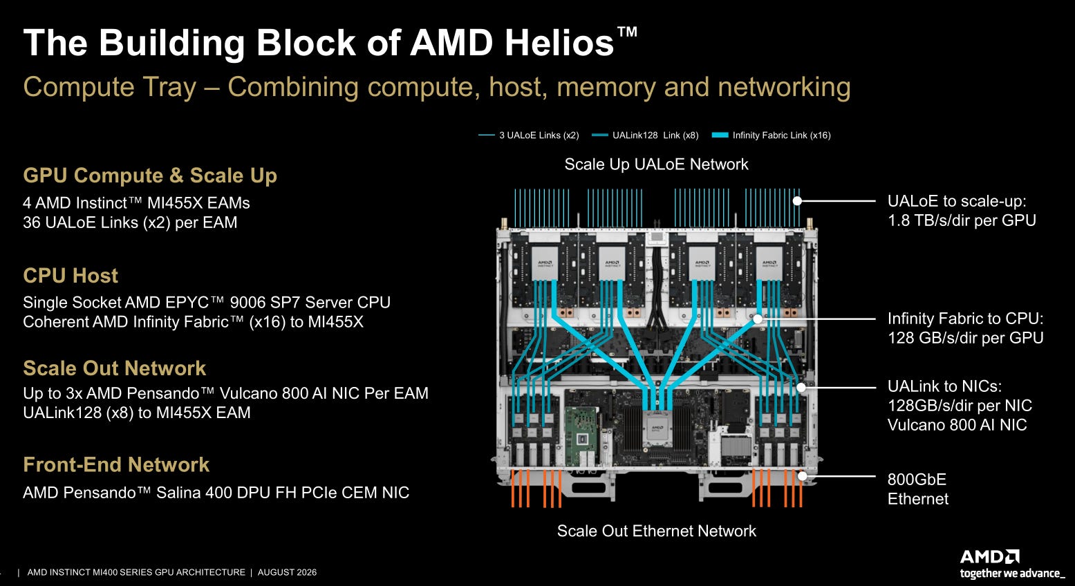
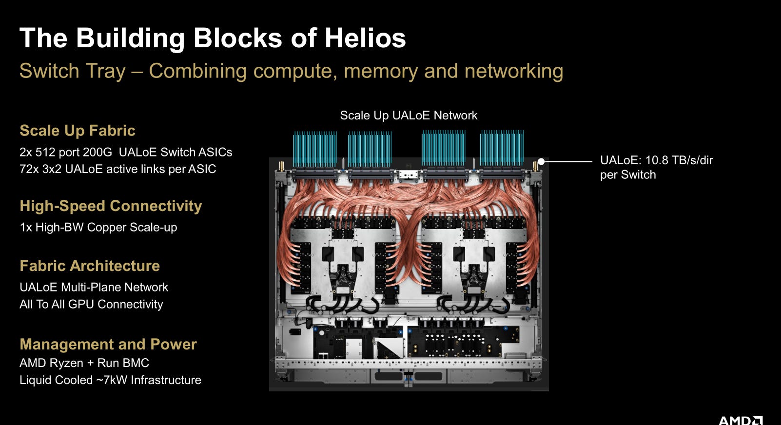
Nvidia just explained why flyover cables are a bad idea. Have fun guys. I am going to be having similar levels of fun next year.
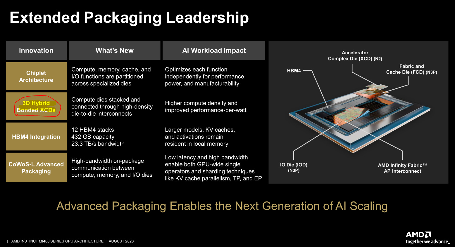
It’s so sad how hybrid bonding is getting adopted (finally) at scale in logic but BESI is giga-omega-fucked because HBM probably never gona go hyb bonding now that de-spec is a thing. I’m not sure we will ever see any generation of HBM at 16-hi or more.
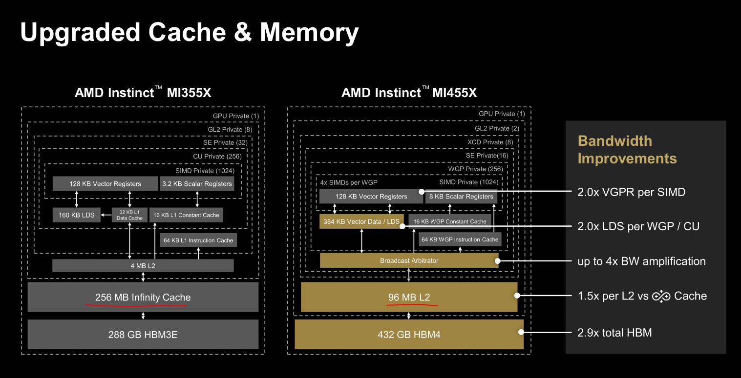
It’s interesting that they decided to prioritize cache bandwidth and latency over capacity. This is an admission infinity cache backfired.
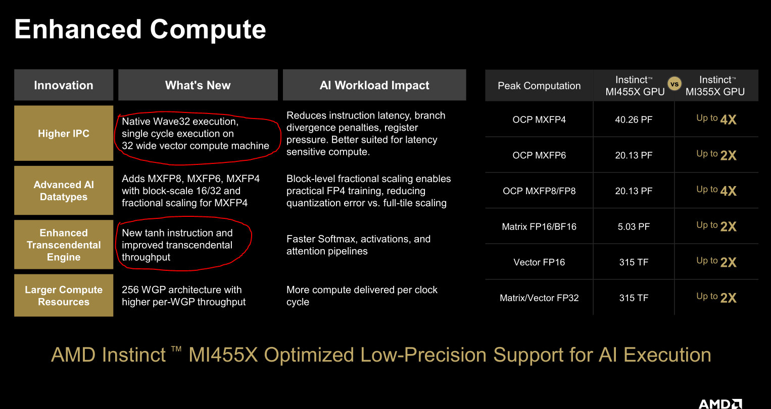
This is so funny. After all these years on wave64, they finally capitulated. Those of you who have followed GPU arch for a long time know how significant this is.
You guys had no tanh acceleration until now? Ouch.
Ah yes another NIC packet performance data. Let me add it to my collage.
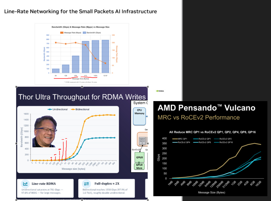
Seems these benchmarks are not comparable. AMD could have shared normal performance like RDMA writes but instead came up with something that makes it impossible to compare with Nvidia and Broadcom. Nice. I’m sure they are not losers and not trying to hide anything.
[4.c] Intel Xe Zombie (please put them out of their misery)
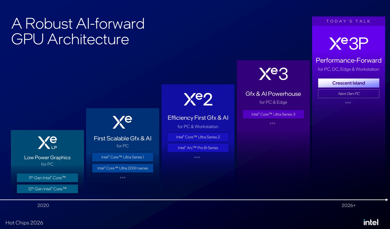
Xe is Raja Koudori’s architecture. He was fired by Pat Gelsinger. Before that, he worked on AMD Vega and Dr. Lisa Su fired him over that.
No human alive has more experience at losing to Nvidia than Raja. AMD GPU group started turning around after Raja was fired lol.
This group at Intel has experienced so many layoffs and re-orgs that frankly the ethical choice is to give them all 6 months severance and eject them.
A big problem in corporate America is this cope ideology of “we have to have a competing solution in this space, it’s too big”.
There is no reality in which Intel GPU group has any meaningful relevance in AI. I can list 10 pre-revenue startups that have a better shot than Intel Xe group. This is not a C-tier program. It’s F-tier.
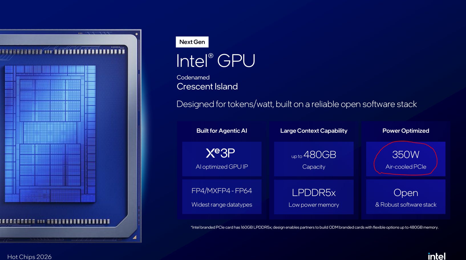
When I think low-TCO token generation, I think air-cooled PCIe card.

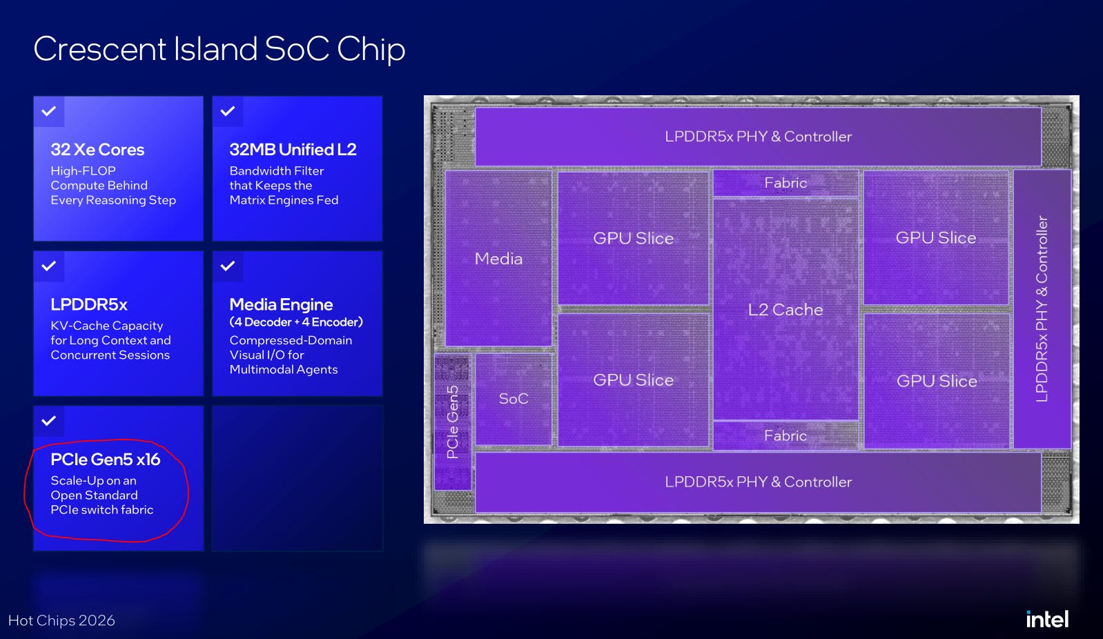
Scale-up on PCIe 5 in 2026. Why the fuck does this exist? It’s actually a waste of sand.
[5] Waymo
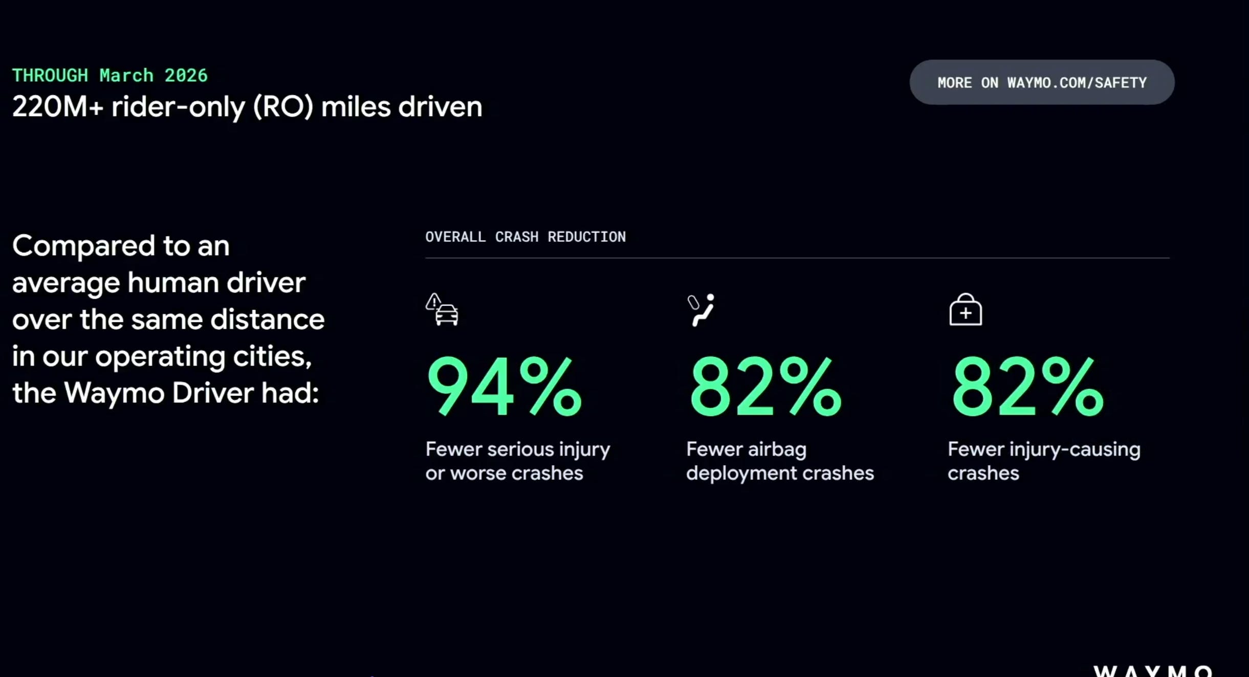
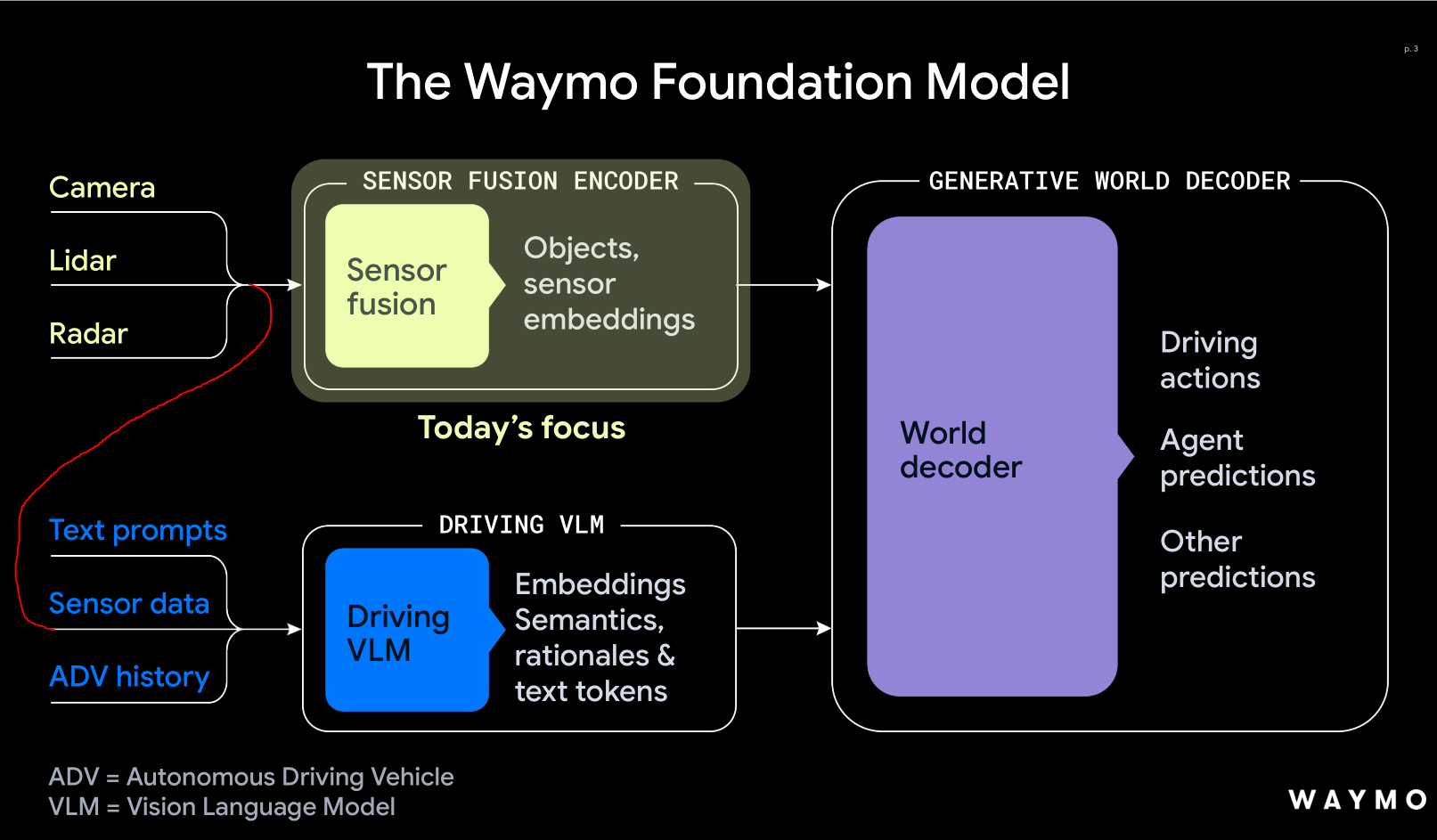
Waymo had a keynote and a technical chip presentation. The keynote slides were not shared because it is full of videos and they want people to see the material as intended. Honestly that’s reasonable I respect that. So… there gona be a lot of screenshots in this section.
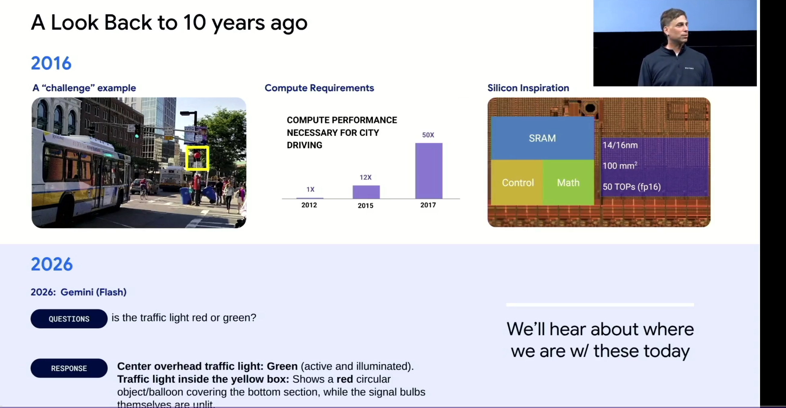
This is a really funny real-world example let me zoom in.

Green traffic light but one of the lights is blocked by a red balloon or something. Conventional conv-nets struggle with this. Generative/transformer models can reason around such scenarios.
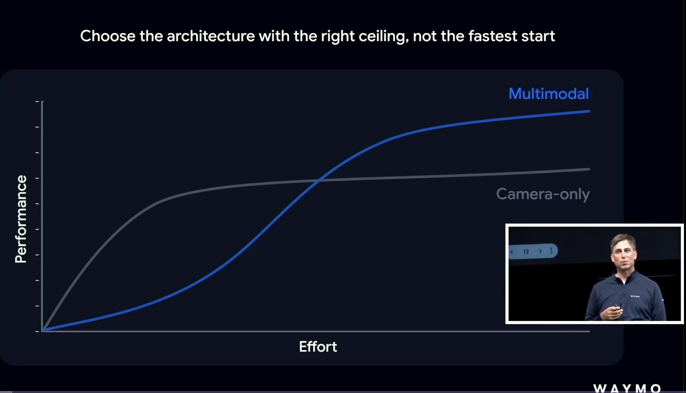
At this point the Waymo presenter took a direct shot at Elon Musk and the argument that humans drive with only eyes/cameras thus LiDAR is not needed.
Waymo’s objective is to make a super-human driver that is far safer and more reliable than any human. To achieve that you need more sensors than just image.
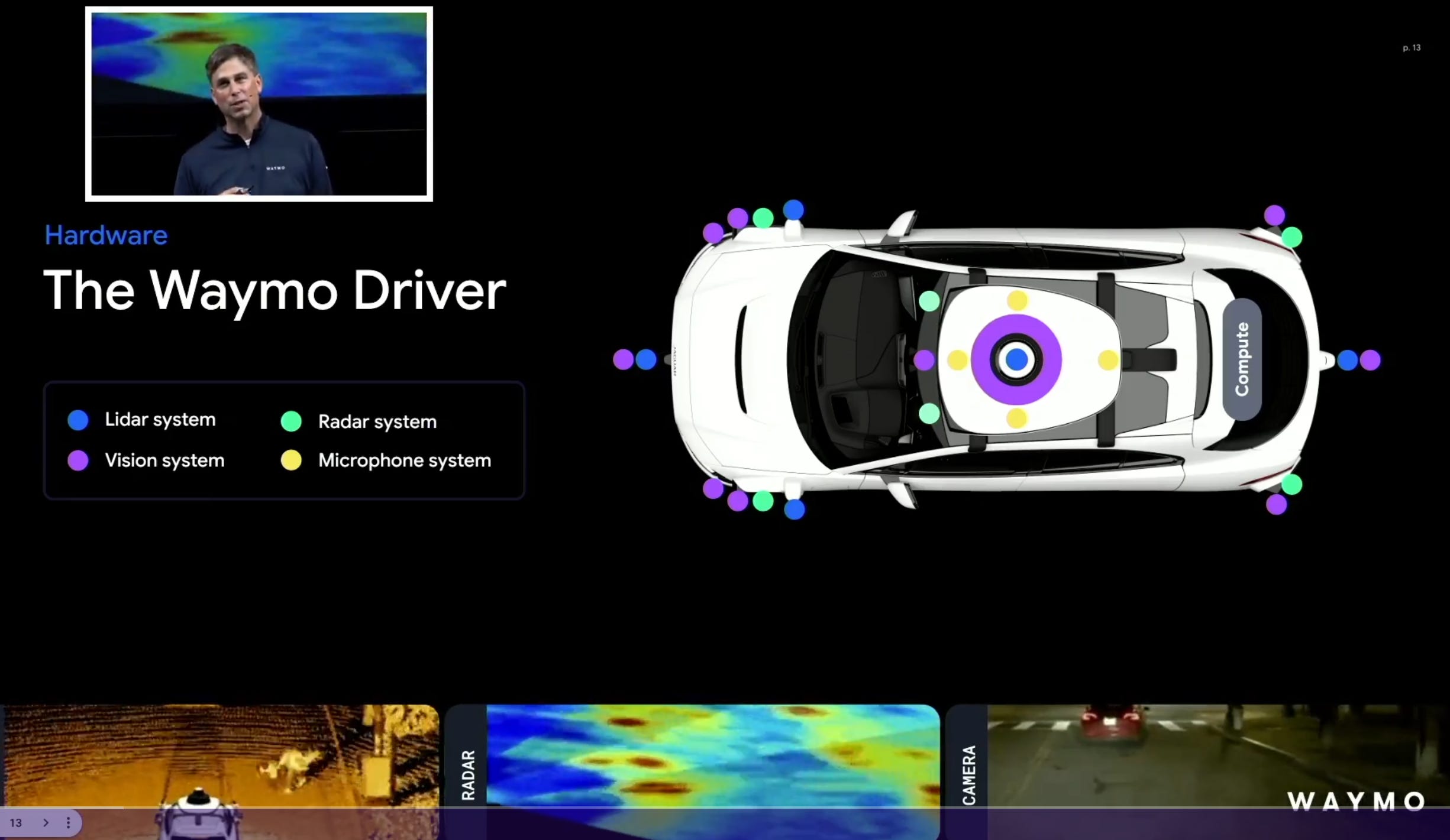
Interesting than microphones are used.
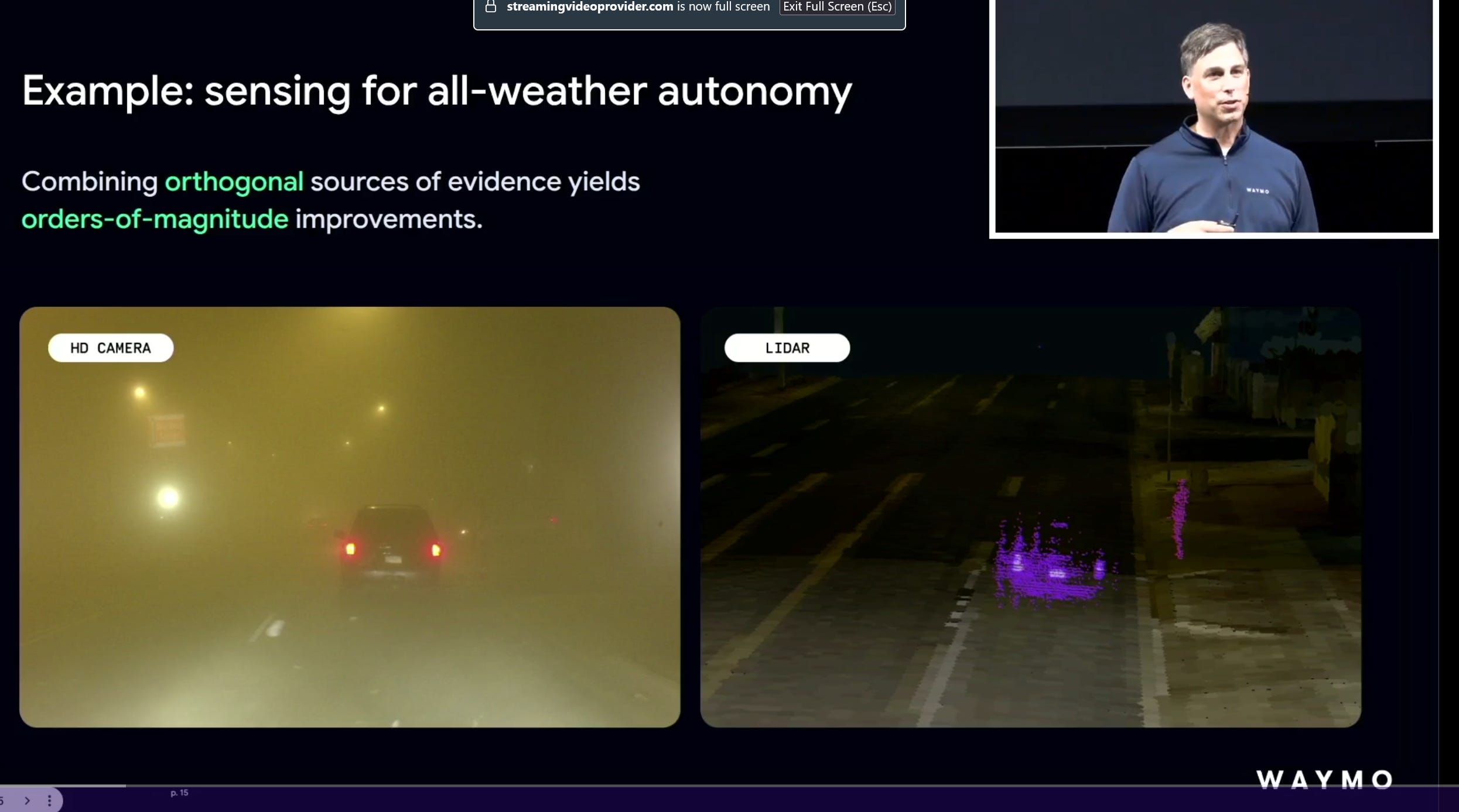
Here is an example where LiDAR helps a lot. Shows an obscured pedestrian.


In this video clip, the Waymo car suddenly jerked to the right then after a few seconds went back to the left lane. Why? Is this a bug?

It’s because some pedestrians were jumping the concrete barrier of a fucking freeway.

I don’t see shit. No human could see this. Wonderful example of the Waymo philosophy of building a super-human driver with all possible orthogonal and complimentary sensors. FYI Waymo makes all their own LiDAR and radar sensors in-house. RIP LiDAR shitcos.
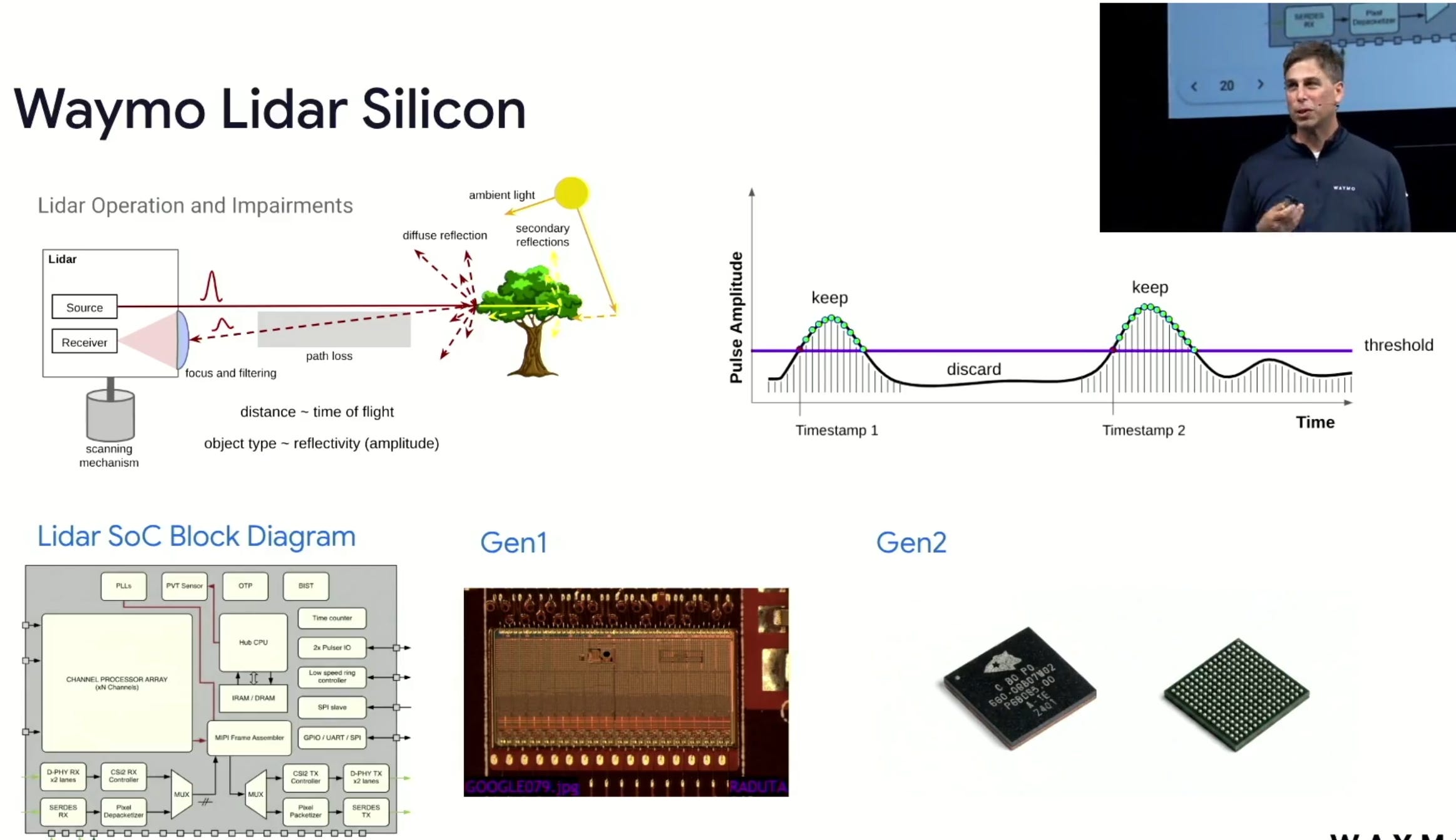
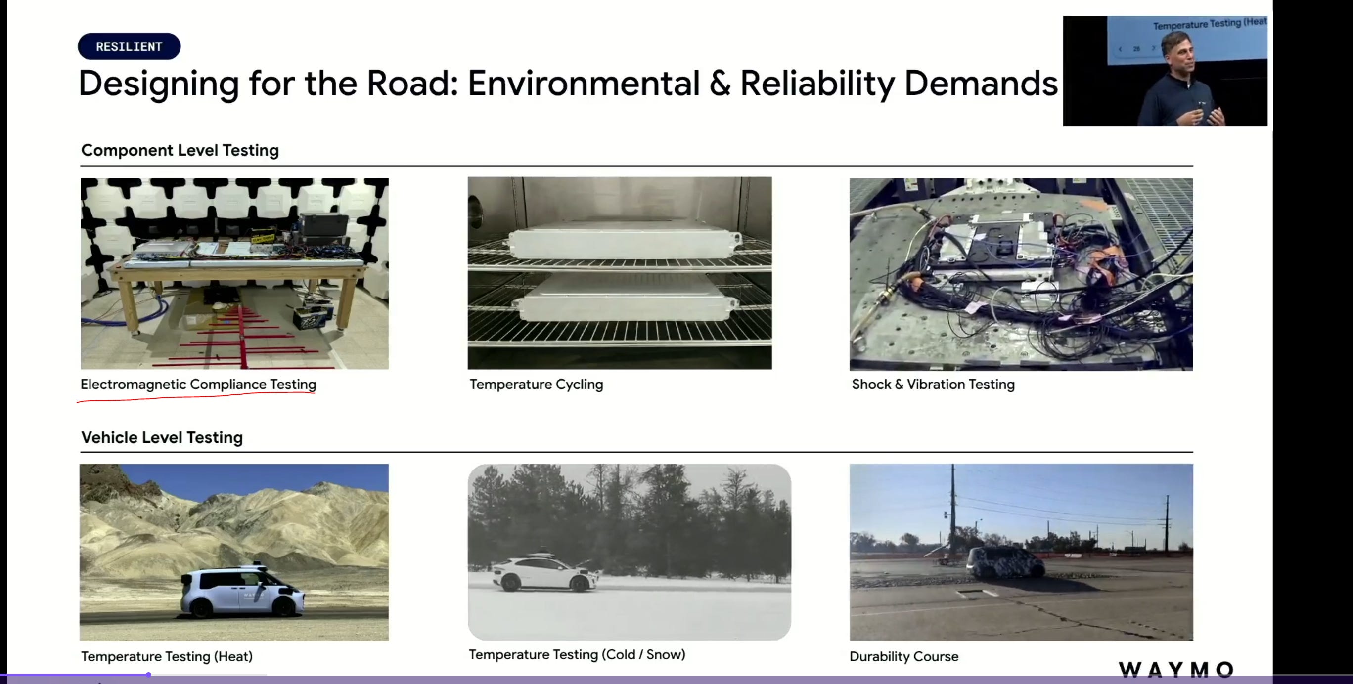
Was initially surprised to see EMI testing but the radar and LiDAR do pollute so makes sense.
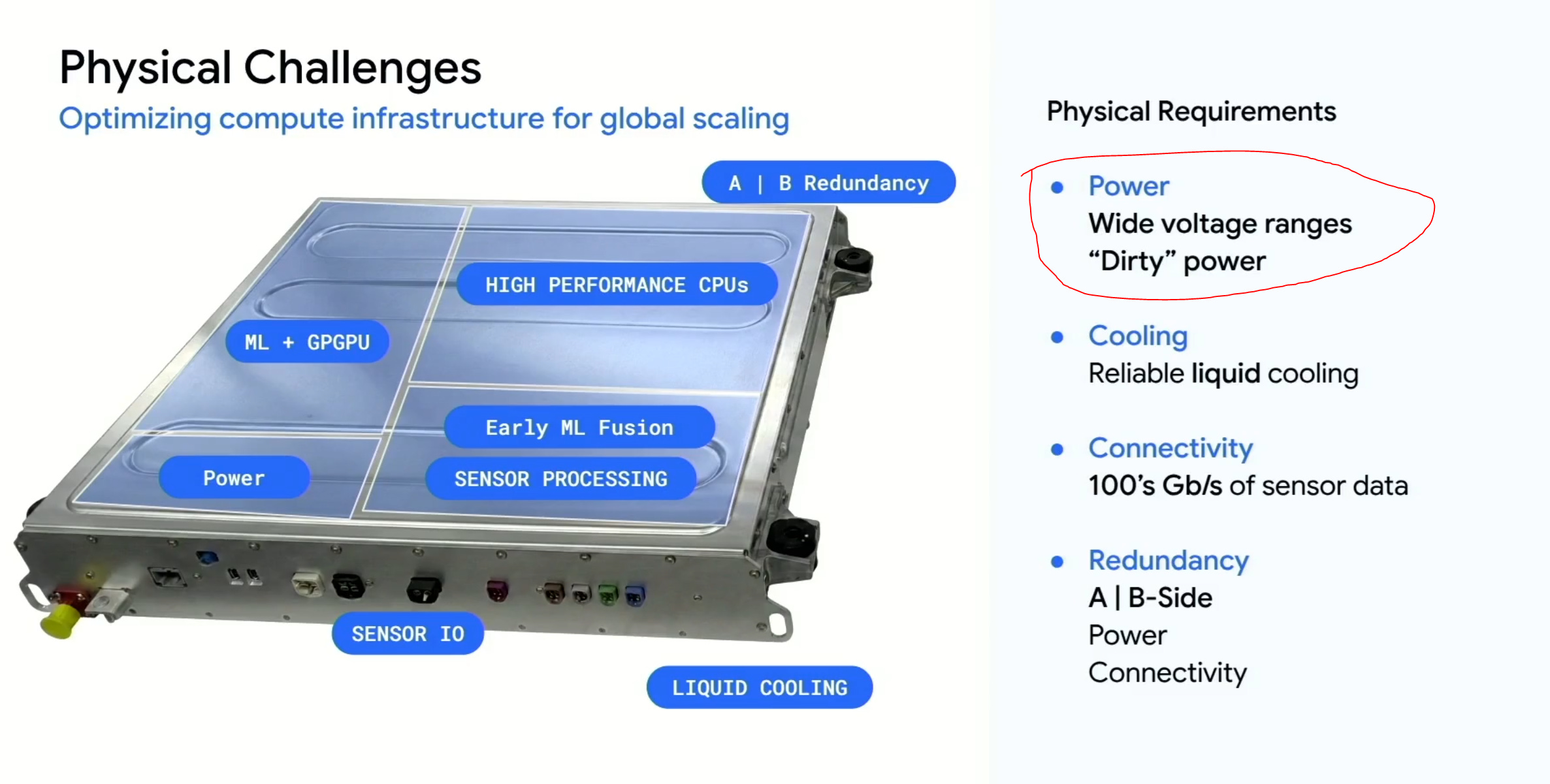
Interesting they design all their chips to be tolerant to ripple. Must be very annoying.
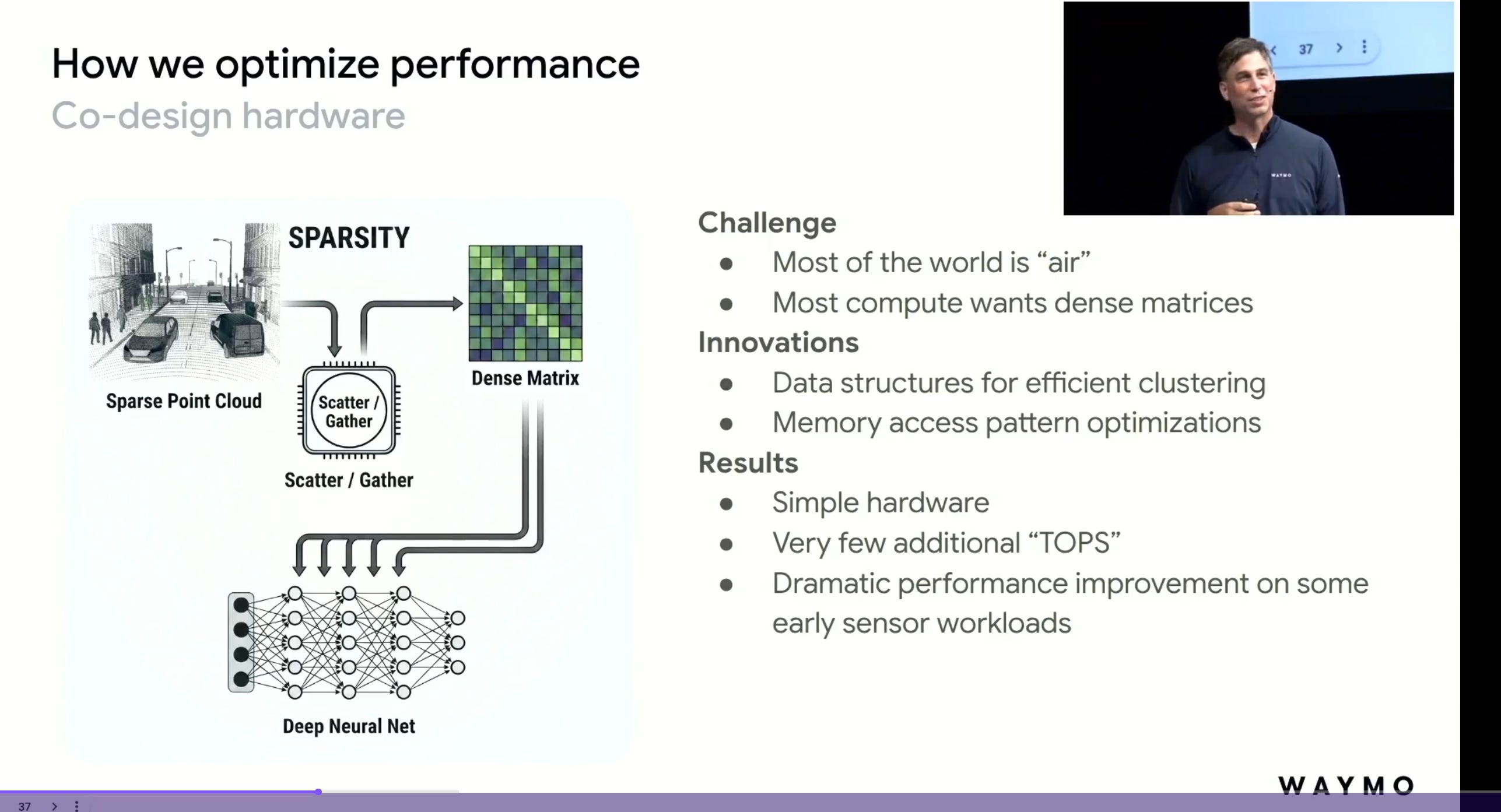
Makes sense that weight and activation sparsity works well given the kind of data they ingest as input.
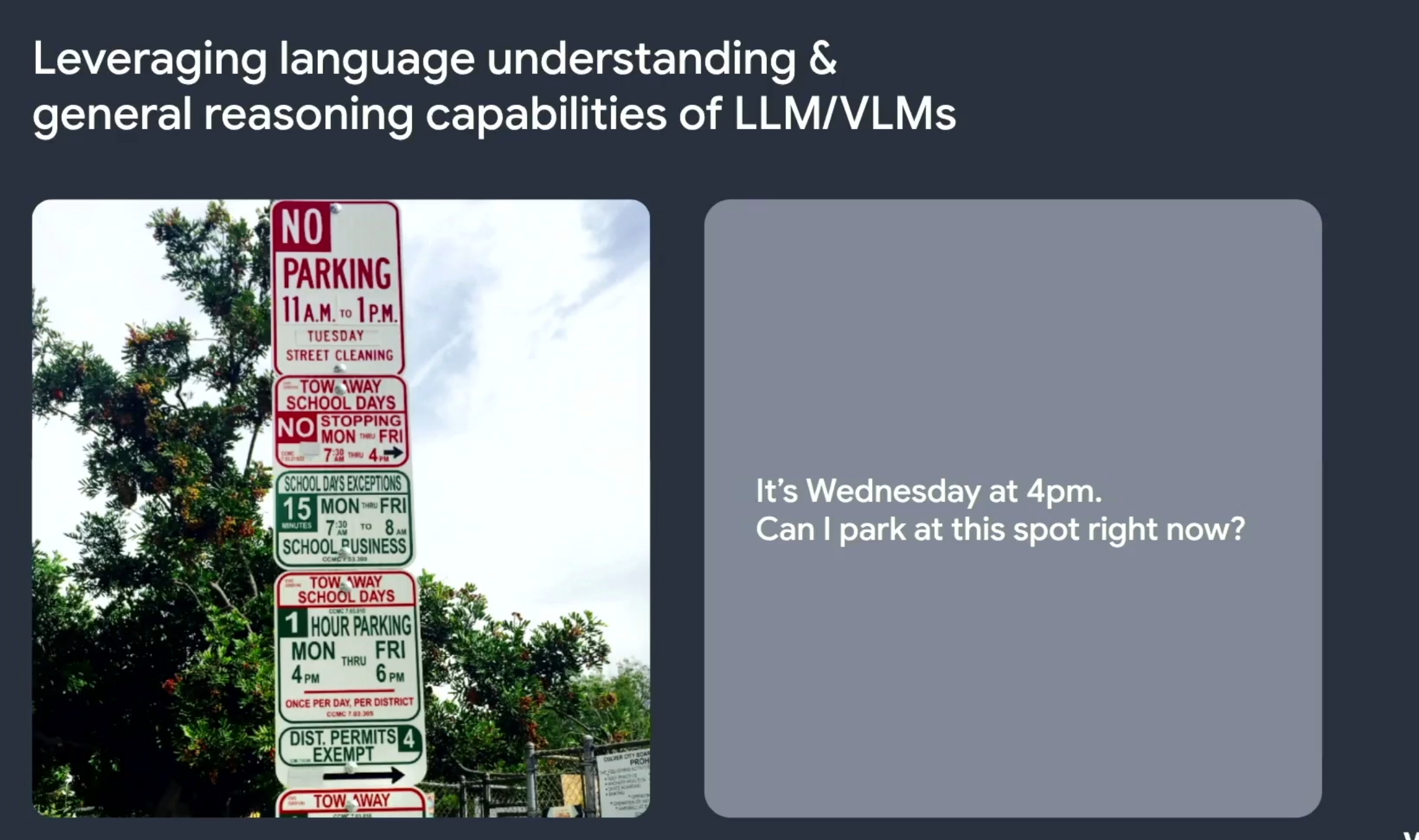
Good point. There was audible laughter in the auditorium at this moment.
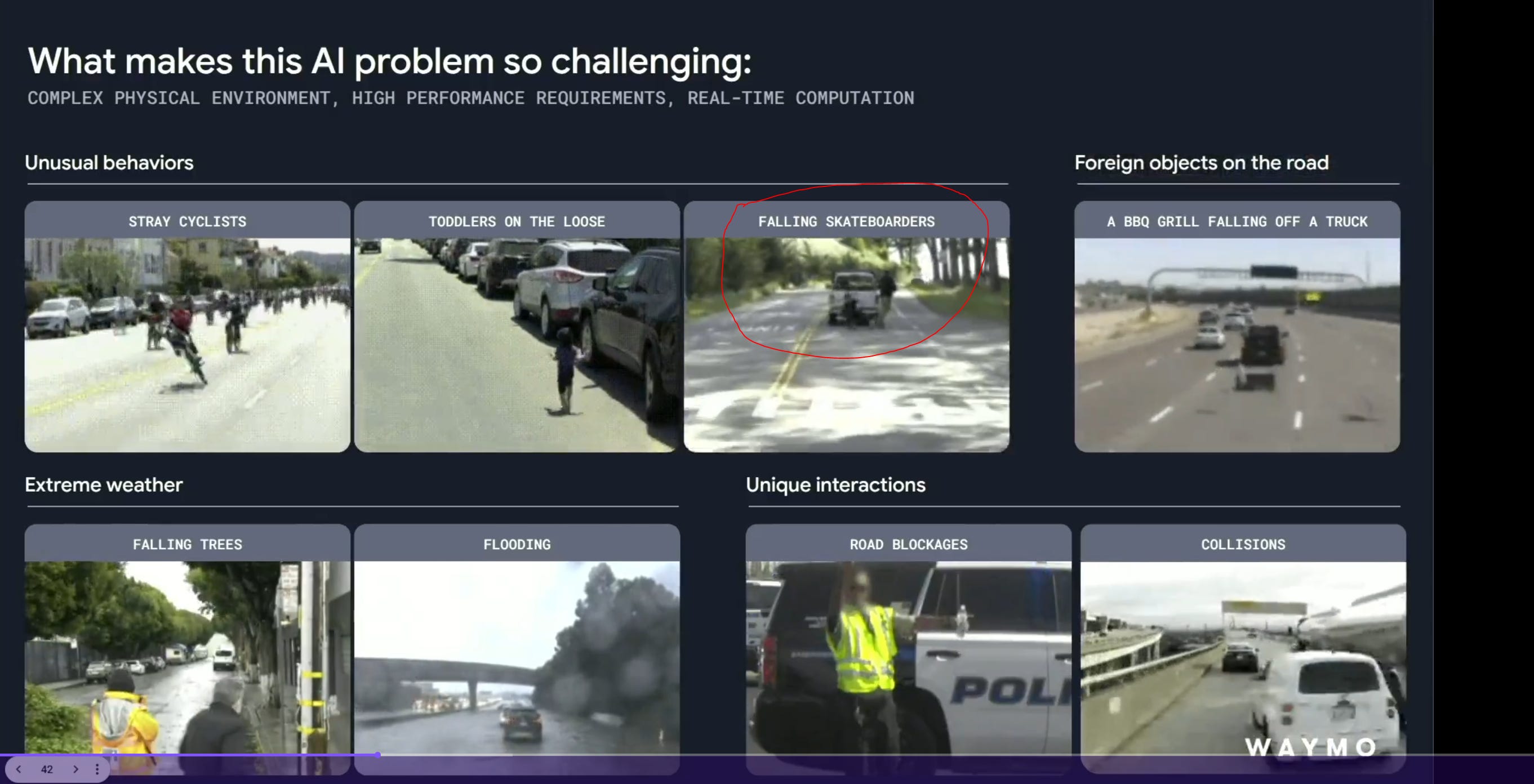
Ah yes. How to respond to skateboarders getting dragged behind a pickup truck for fun and falling off. EDGE CASES



They have a pretty good world model/simulator. Snow on the golden-gate bridge.
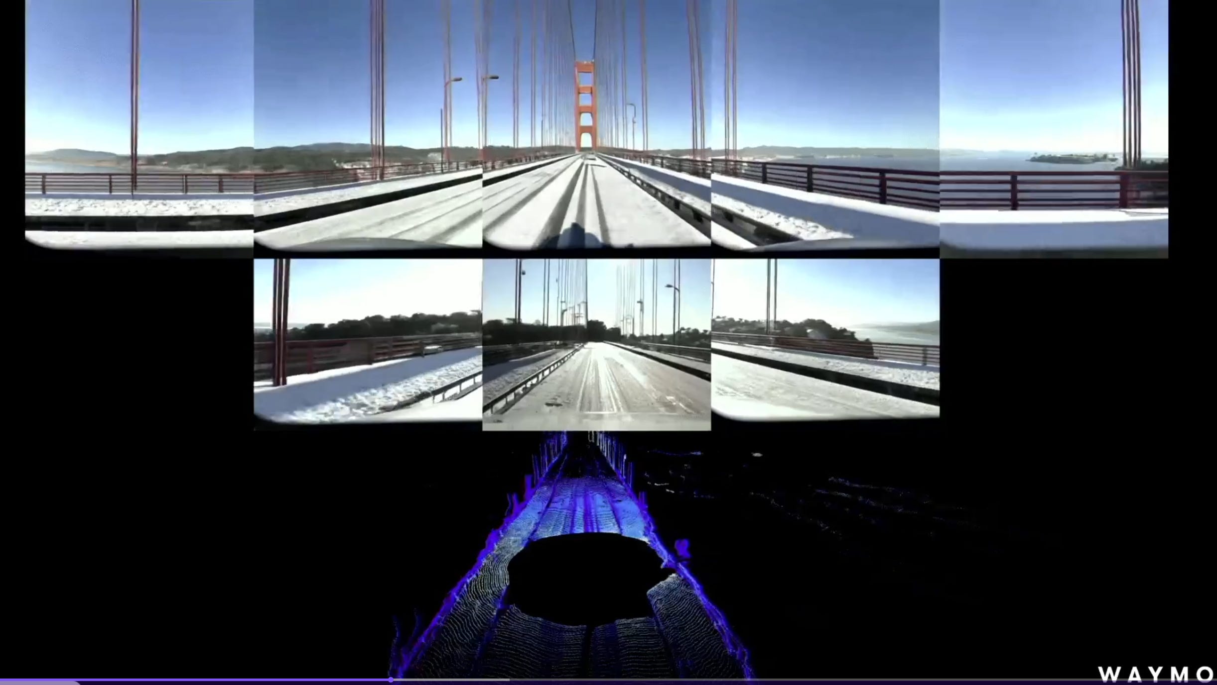
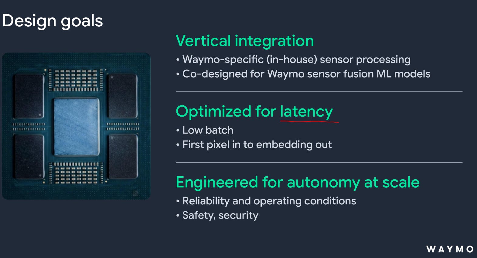
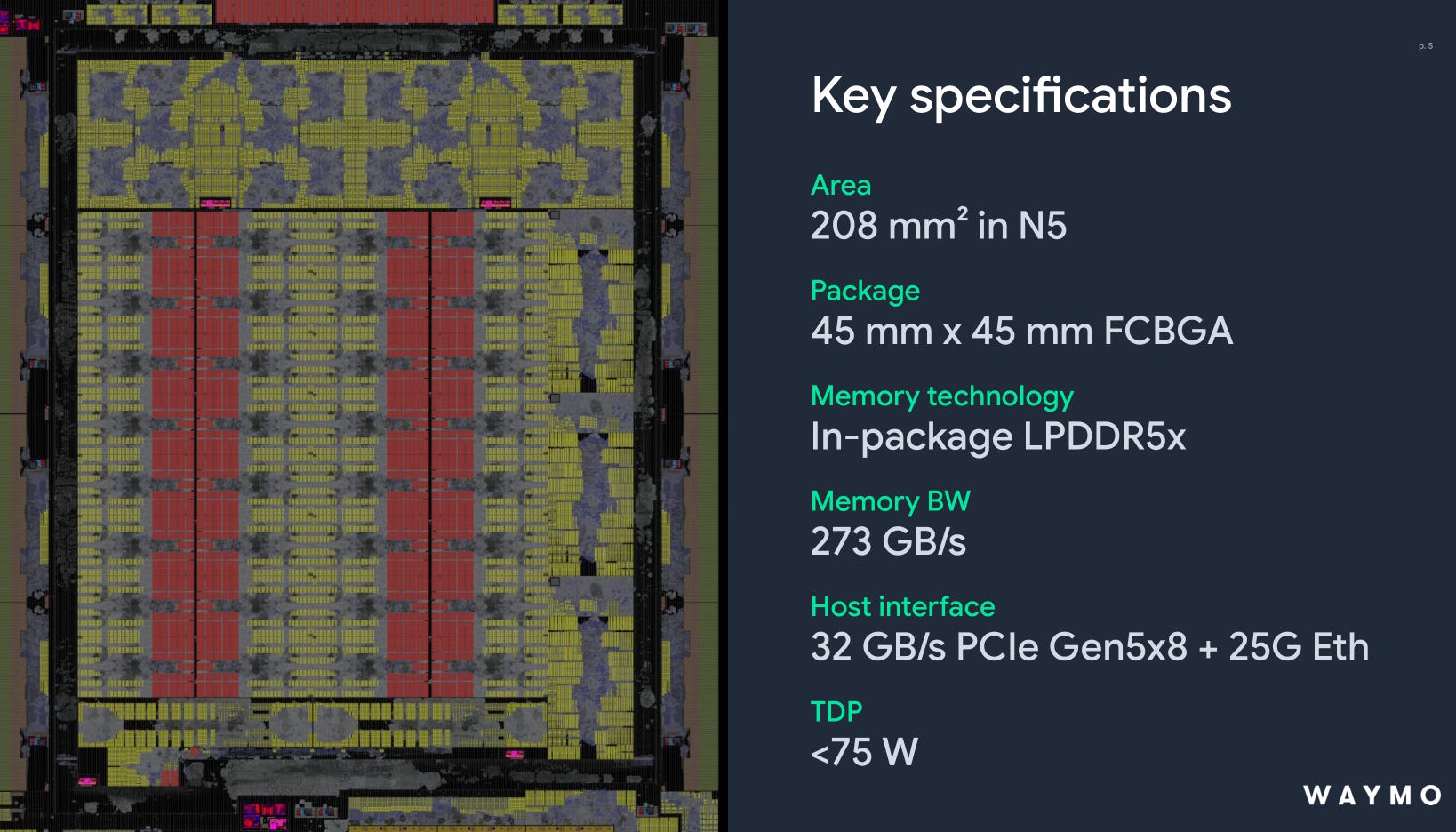
Keeping embedded chips under 75W is a typical goal as that is PCIe card power limit using a standard CEM connector.
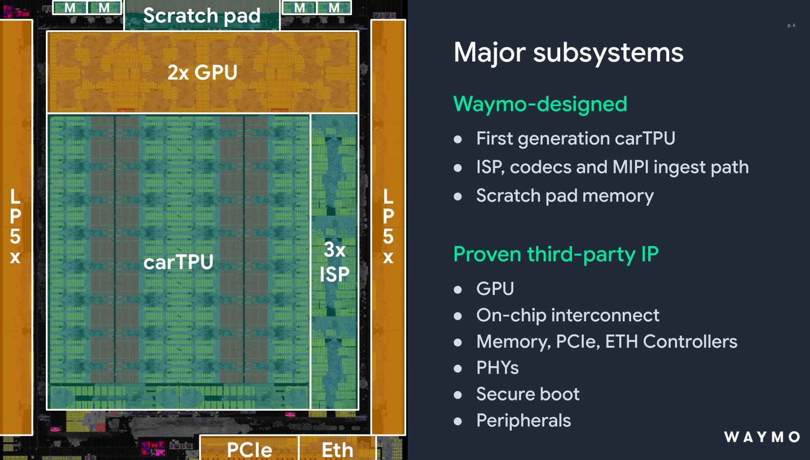
They did not specify where the GPU IP is from. It’s either Imagination or ARM. Both are trash but whatever.
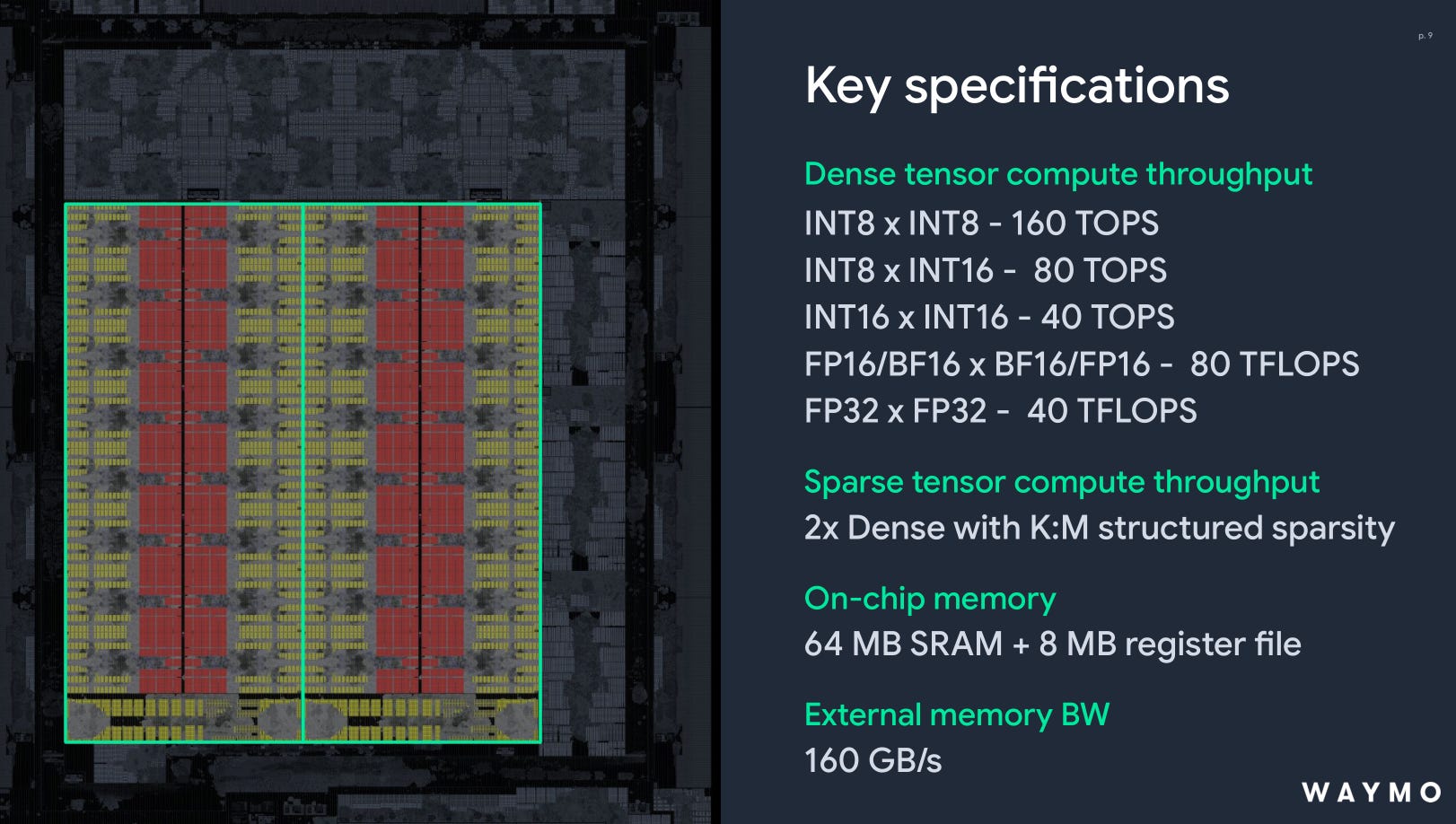
The high-precision (FP32) support/focus is because they process a lot of high-resolution camera data.
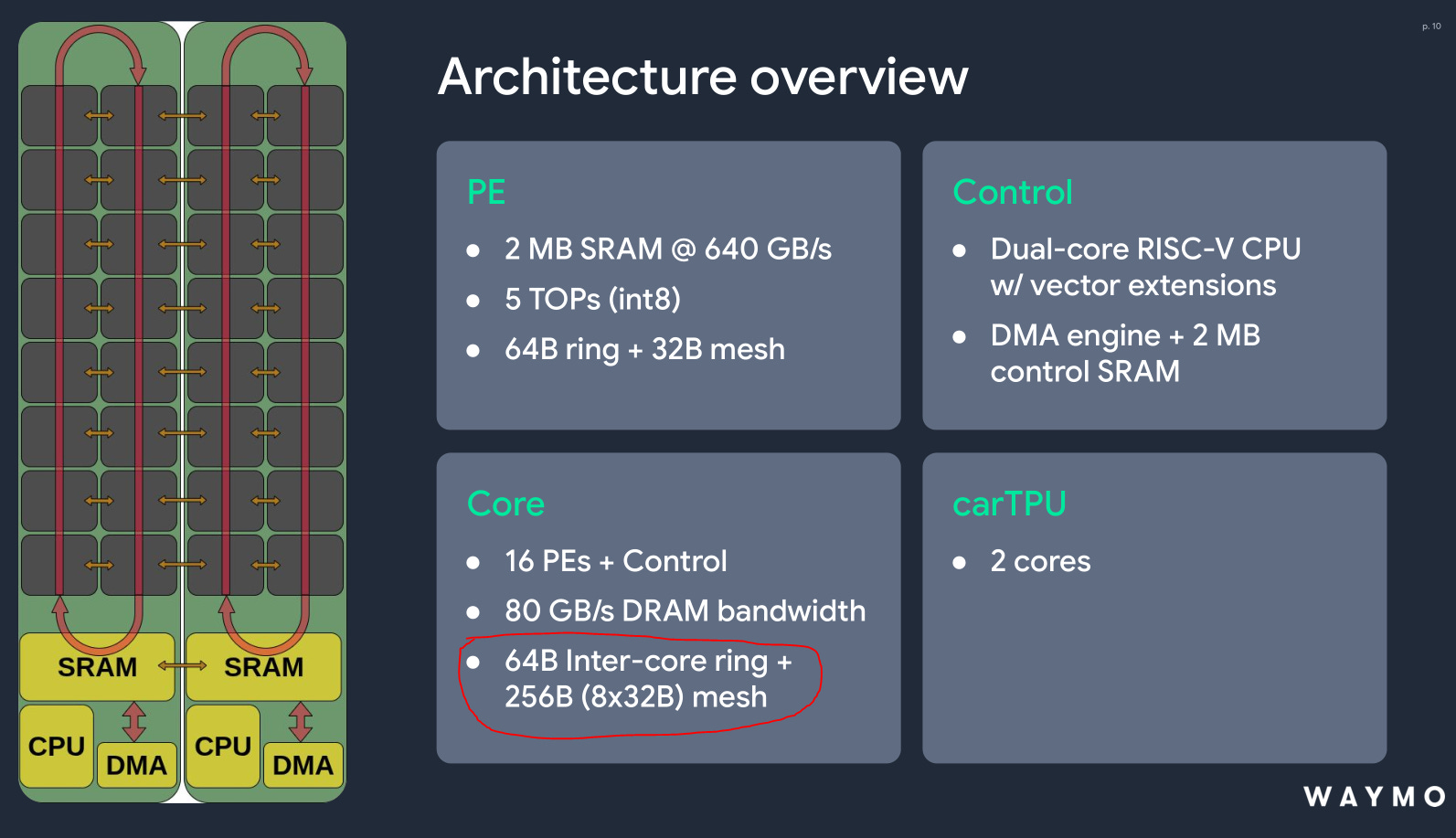
NoC topology is interesting. Mesh for horizontal, a quite wide (unidirectional?) ring vertically. Weird access patterns in exchange for better power efficiency.
They say latency was an important design goal but this NoC is kinda terrible for latency unless it is programmed optimally. Interesting.
“The [RISC-V] CPU just acts as an orchestrator.” Once again, RSIC-V fans hope for relevance in high performance or userspace is dashed.
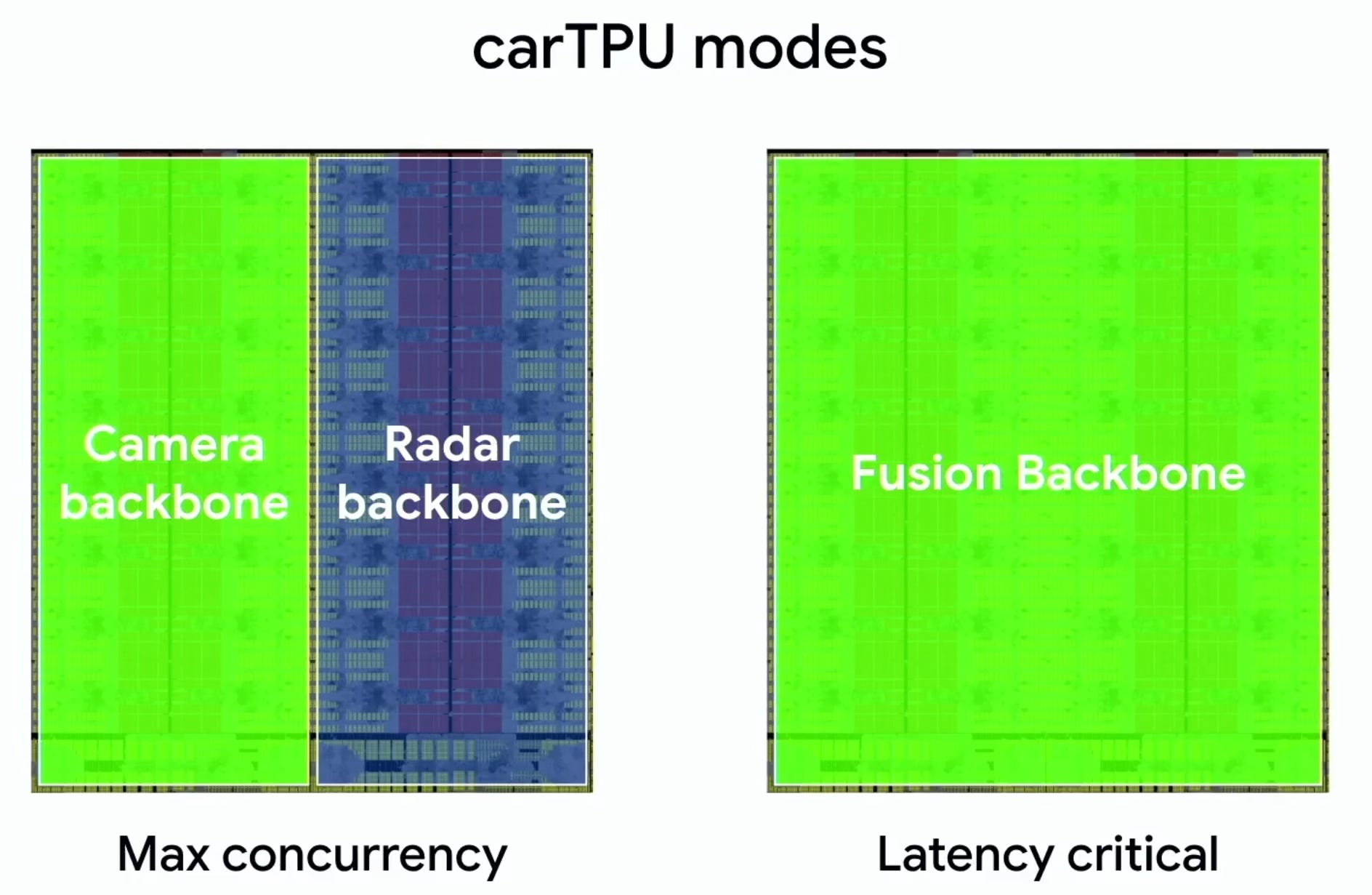
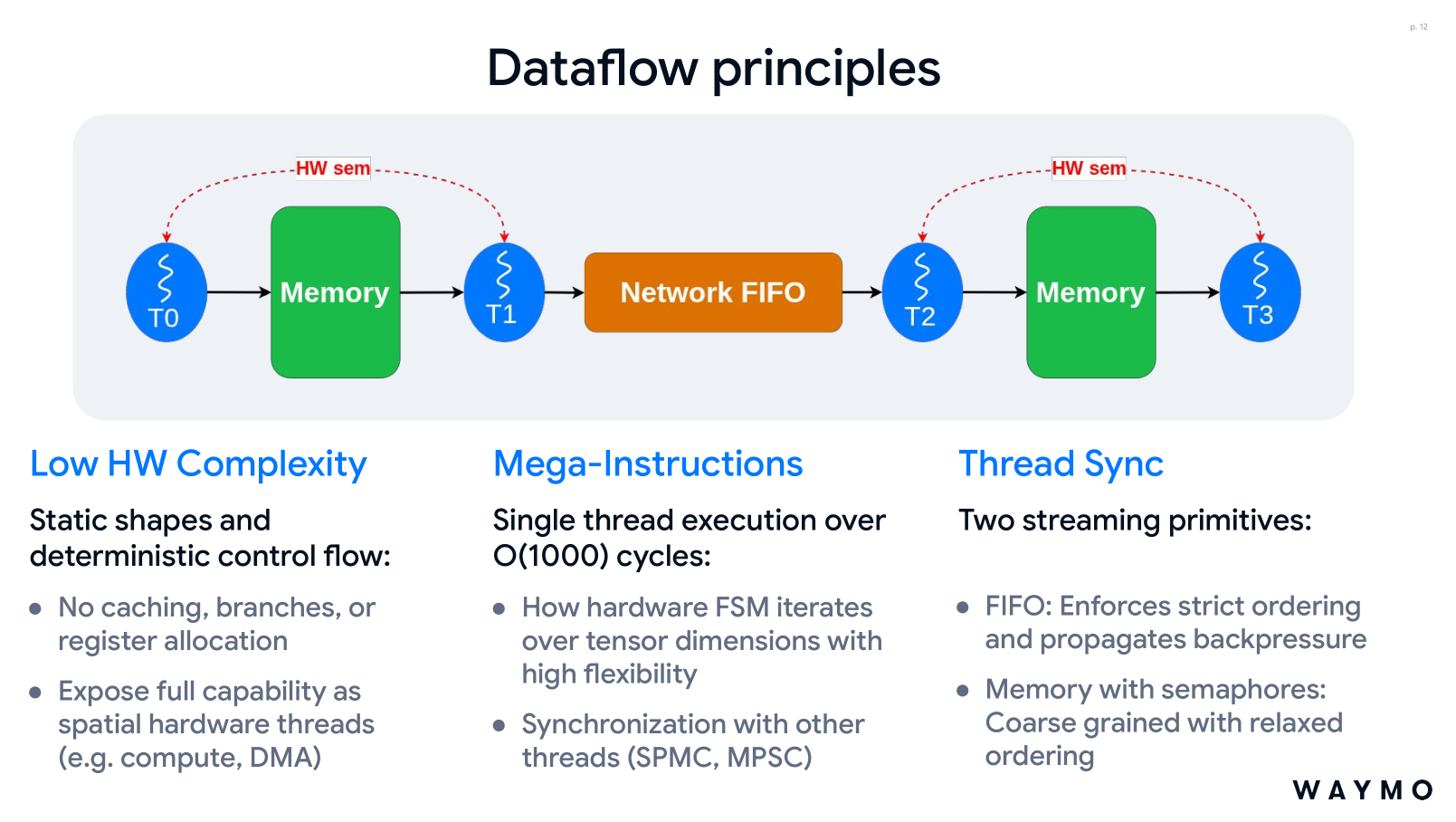
Two cores (16 PE each). Either separate tasks or fuse together to perform one latency-critical task. They also easily dump in-progress inference tasks to DRAM in order to prioritize latency critical tasks that show up unexpectedly. Clever.
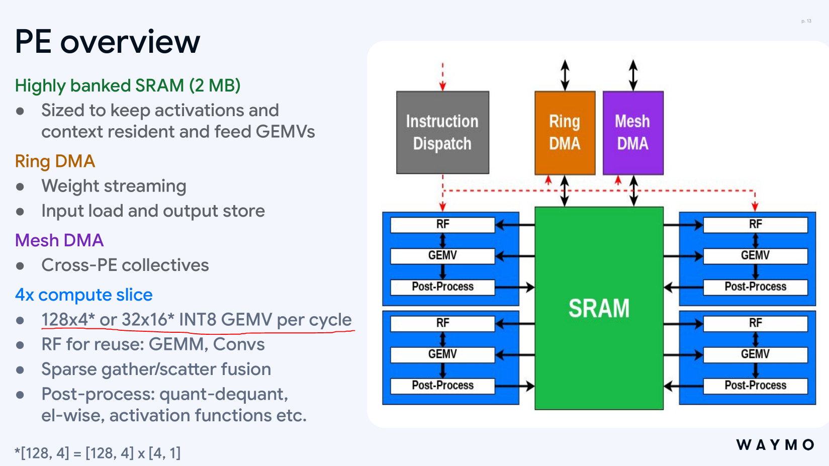
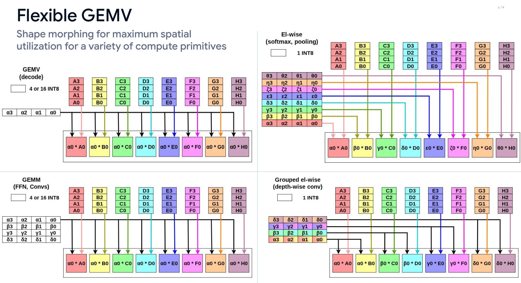
The shape of their matrix-vector multiply units is interesting. Quite tall. The use the register fire (RF) to enable larger matrix operations. Wonder why they care so much about small ops. It is unusual to make the systolic array so small and so rectangular/tall.
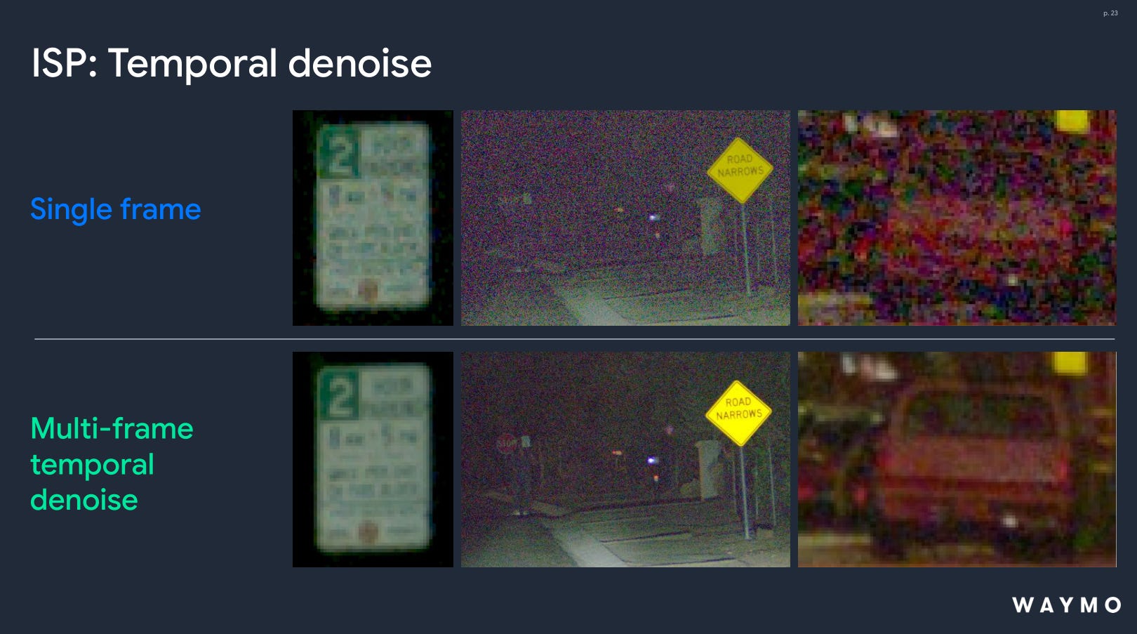
Interesting temporal de-noise. I wonder if discrete-cosine transform involved.
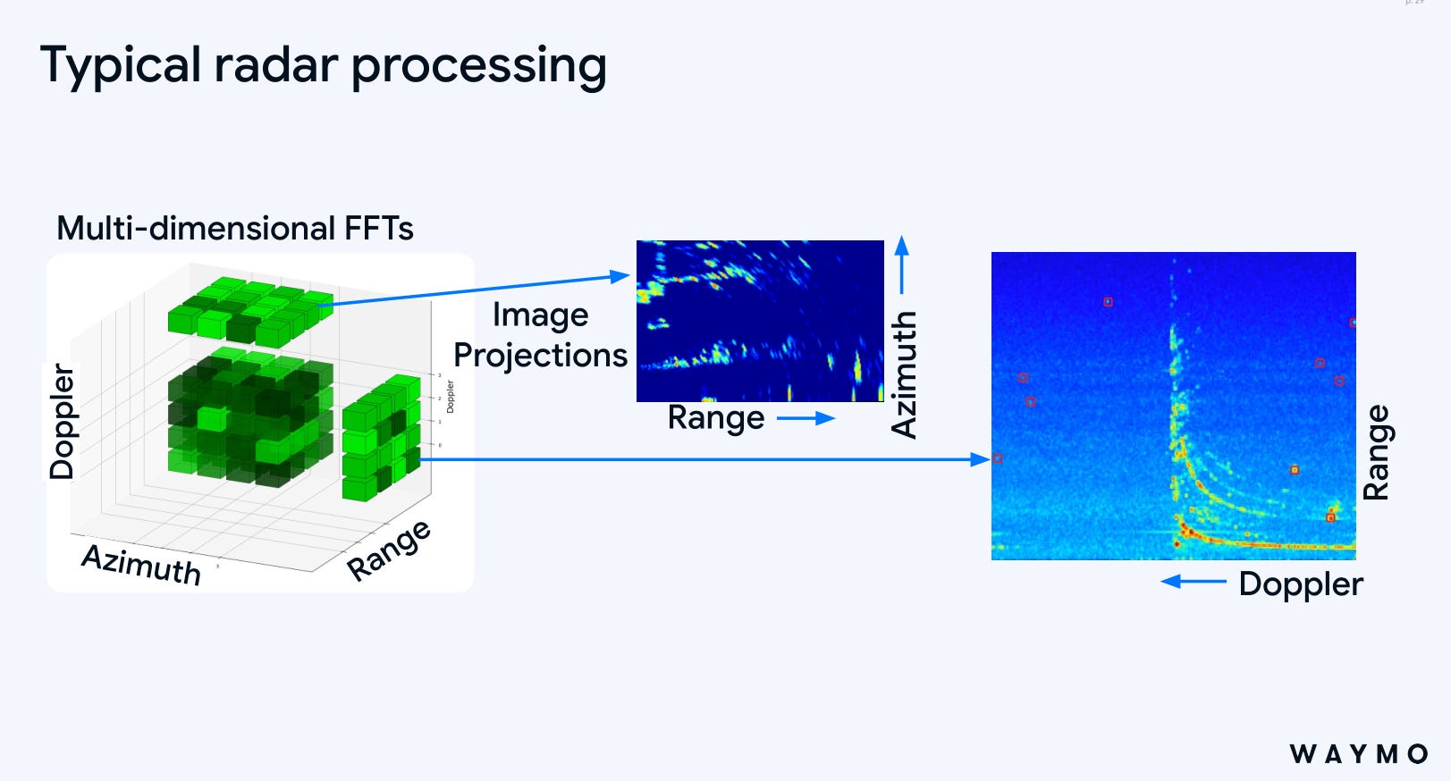
Curious on what size their FFTs are and windowing strategies.
[6] CPU (real ones not RISC-V garbage)
This section is for all the interesting CPU talks. By far the best one is the IBM one.
The RISC-V losers get their own section.
[6.a] IBM Galaxy-Brain Dual-ISA Mainframe-Grade CPU
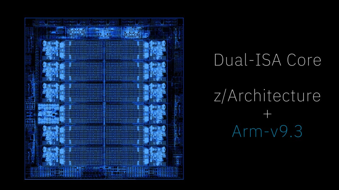
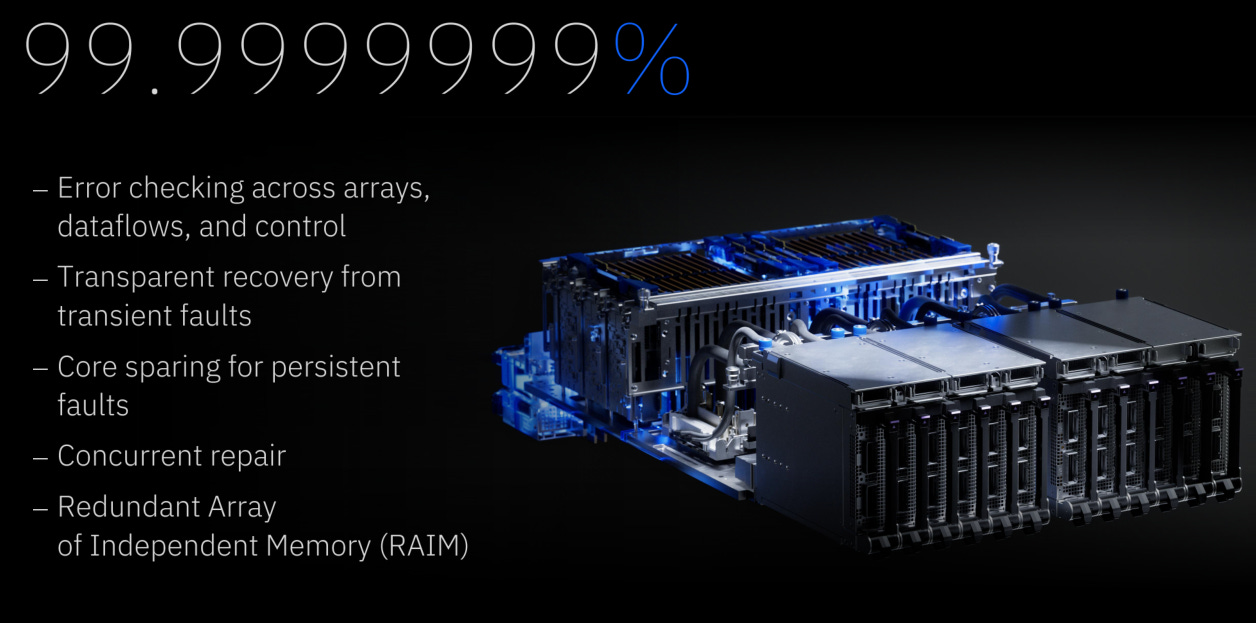
IBM Z is the mainframe line. Designed for ultra-high reliability. The typical customer for this is banks (transaction processing) and infrastructure providers. Think government/military/healthcare/utilities databases.
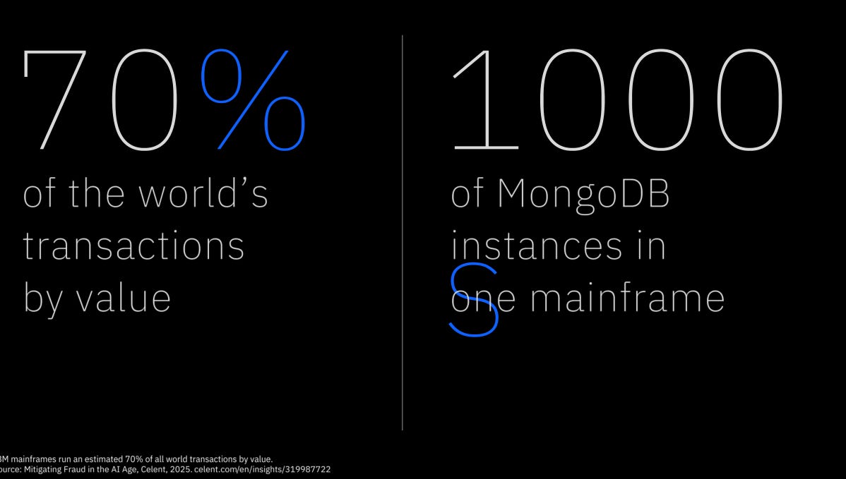
The Z instruction set is CISC and (effectively) proprietary to these captive customers who need the reliability and cannot use anything else.
From a business perspective, it makes sense for IBM to make their TAM much bigger buy adding ARM V9 support.
From an engineering perspective… this is insanely cool. Nobody has ever made a full-performance dual ISA CPU. AMD tried a long time ago with the K12 (x86 + ARM V8) but killed the project because they were going bankrupt.
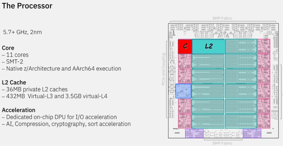
36M of L2 cache per core is massive. IBM also has a trick where they enable L3 and L4 cache to be virtual by combining unused L2. This is something unique to IBM Z. The typical setup is private L2 and L3 or shared L2 no L3, or private L2 shared L3.
Each SMT thread can switch between Z-mode and ARM-mode at runtime.
On-chip DPU is similar to what AI accelerators like TPU do. No switch, just have the in-line data processing on each chip.
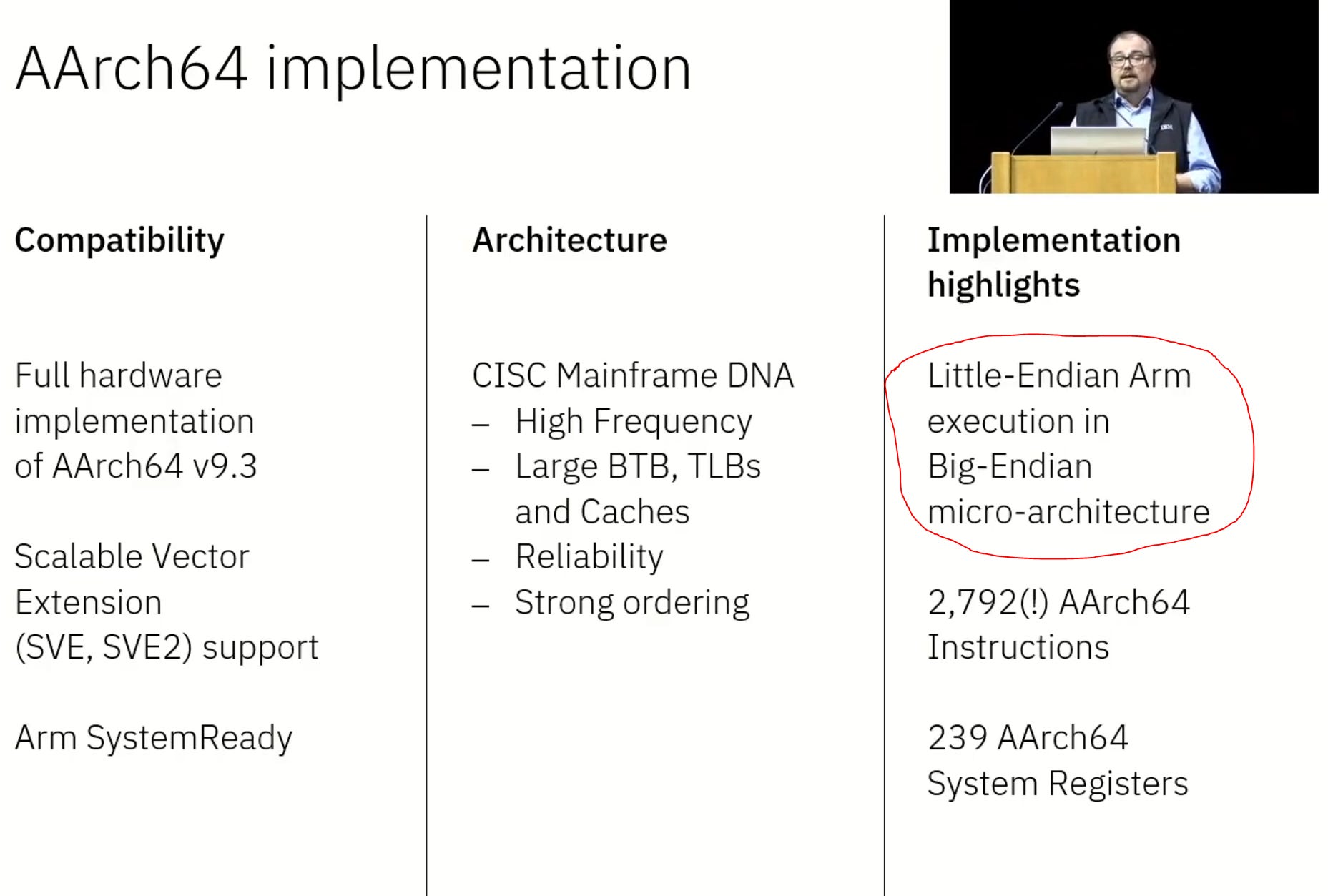
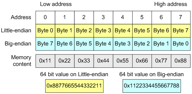
Getting ARM to run on a microarchitecture designed for big-endian and making software obvious to this is a huge accomplishment.
Ironically, the CISC Z instruction set has half the number of instructions at Aarch64, a RISC-style ISA.
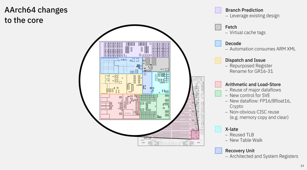
Decode had the most changes.
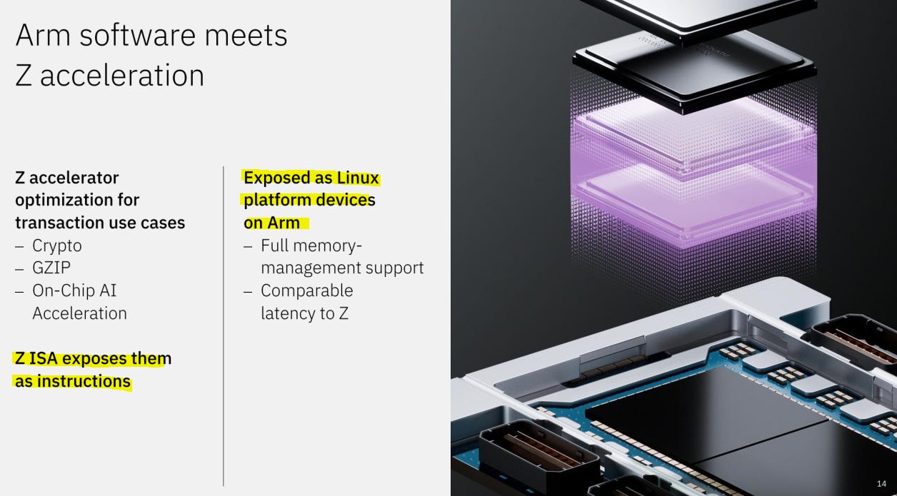
Many useful Z-ISA acceleration instructions are transparently exposed to ARM software using standard Linux hooks. Linux sees these Z instructions as fake devices, the same way Linux views a USB device.
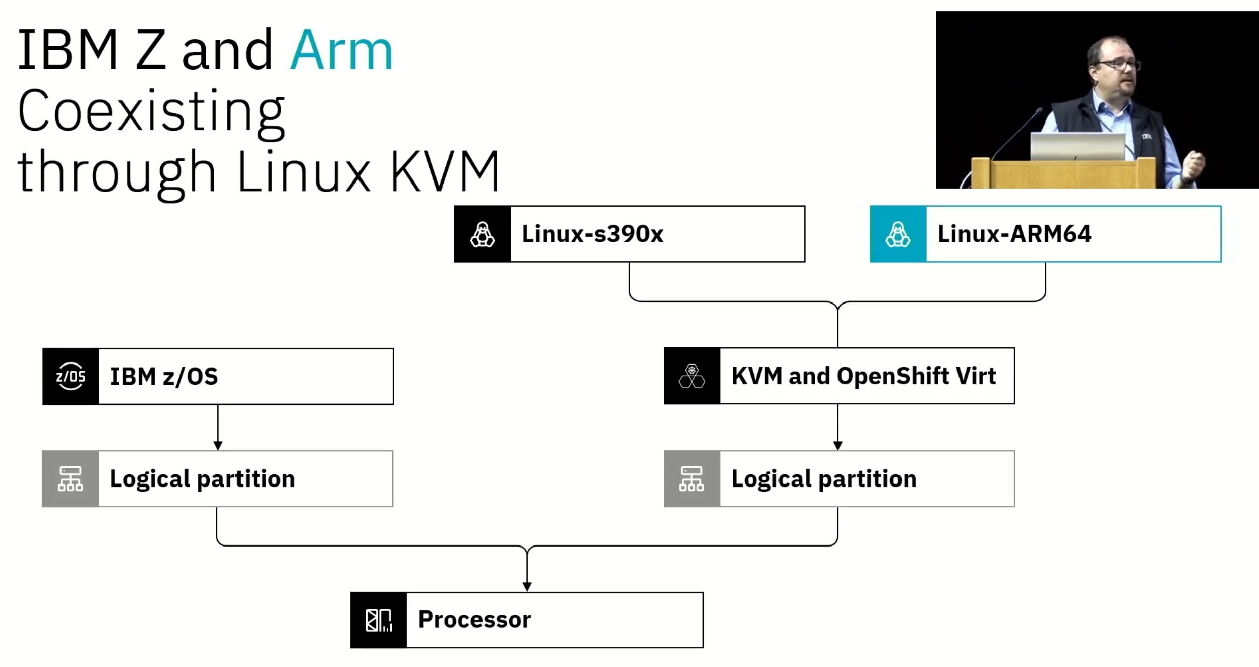
It only takes nanoseconds for the hypervisor (KVM) to switch between ISA using two existing Linux instances.
IBM added a new CISC instruction in Z-ISA to enable the switching. This has already been upstreamed to the Linux kernel.



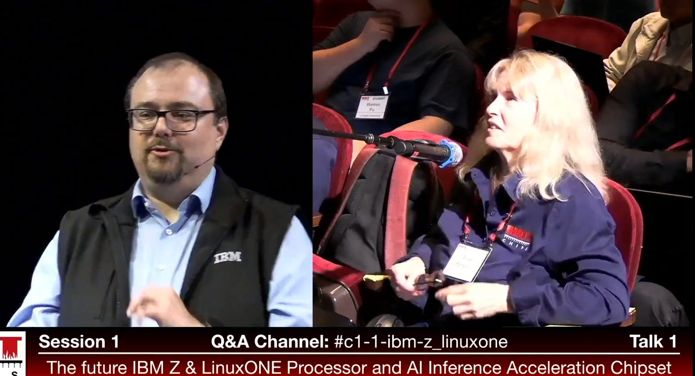
“No other ISA made sense for this endeavor.”
Thanks for confirming that RISC-V is so useless it was not even considered at all.

Bow to the ISA king, RISC-V peasants.
[6.b] Nvidia Vera (is not complete garbage like Grace)
Before covering Vera, some context about Nvidia Grace is necessary.
Grace is a legendary chip here in the Bay Area. I have literally been to multiple parties where a cluster of AI programmers are gathered to shit on Grace. This chip is so bad, it became a conversation topic.
There is a hyperscaler that literally (not joking or exaggerating) had an internal engineering lecture series on “why Grace is bad and how to write code to get around this shit chip”.
Grace had two main problems:
The ARM Neoverse V2 core has a critical design flaw associated with the front-end. Don’t remember if it was branch target buffer being too small or something else.
Nvidia chose to use their own internal NoC (network on chip) instead of the excellent ARM CMN NoC IP. Apparently this NoC was and old Mellanox design and is shit.
Vera solves both of those problems. Nvidia made their own core design instead of migrating from ARM Neoverse V2 to V3. They also updated their NoC from dogshit to good.
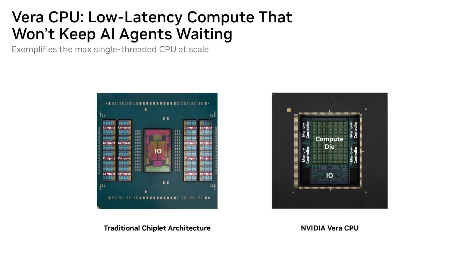
Intel tried to make this argument against AMD back in 2017 and ate shit for years. This is a very annoying strawman argument.
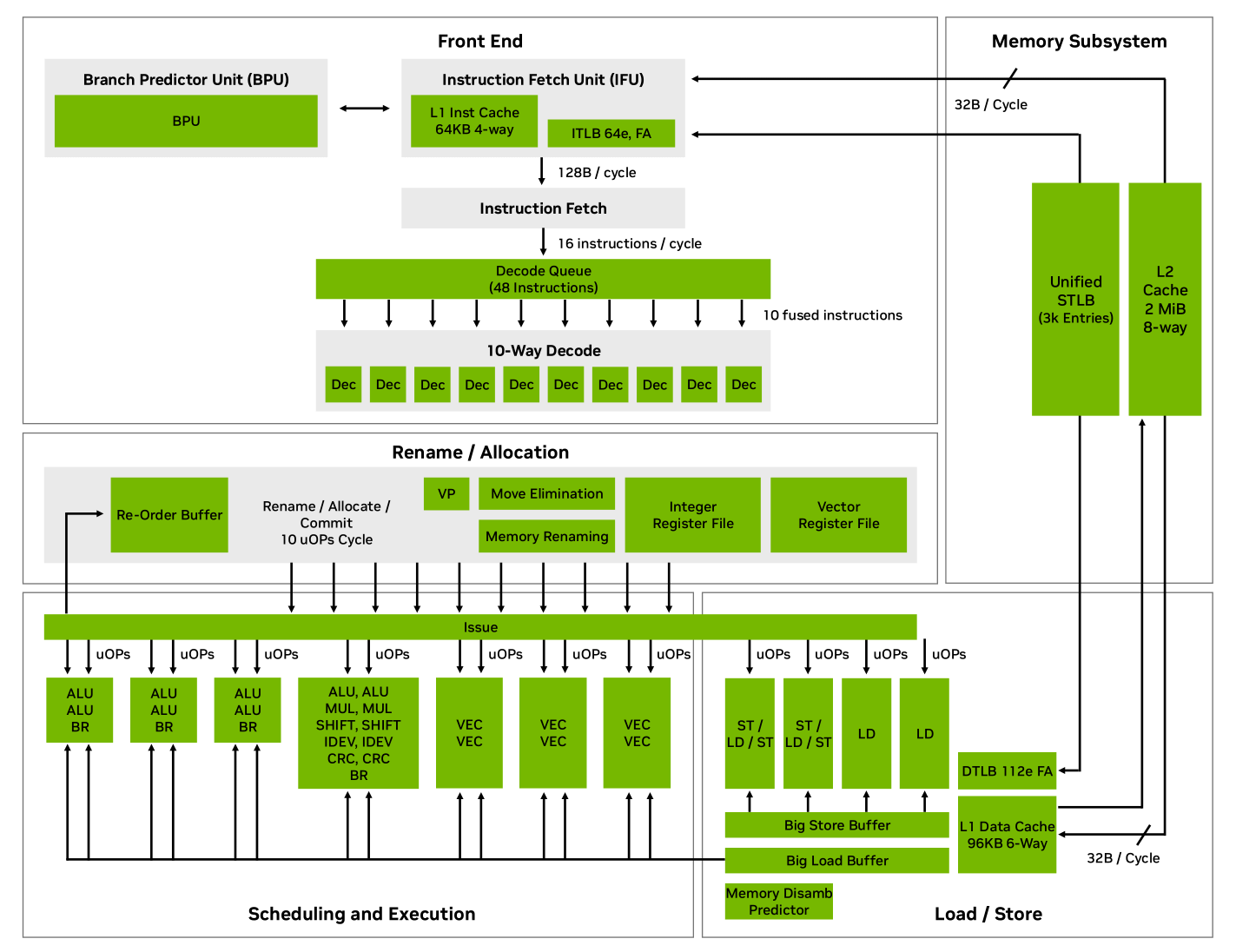
Neoverse V3 is also 10-wide decode.
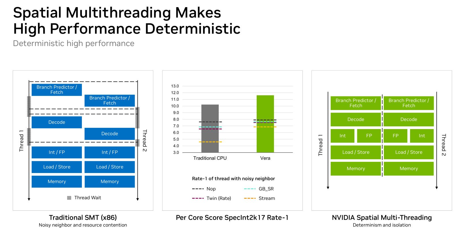
This slide pissed-off a lot of CPU enthusiasts. Normal hyperthreading does not duplicate decode and branch/fetch for good reason. There is usually no point. Nvidia is basically duplicating everything and calling it “spatial multi-threading”. Noisy-neighbor issue is usually from thermal crosstalk (neighboring cores/VM drawing more power) and shared L2 or L3 cache competition. To me this looks like cope from Nvidia.
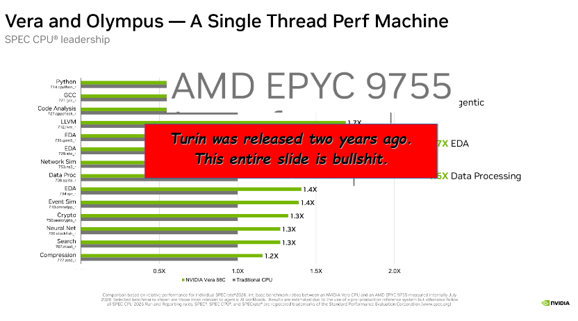
Nvidia is bullshiting with this benchmark slide. Many large Nvidia customers are asking for Intel x86-based NVLink Fusion CPUs over Vera. That tells you all you need to know about Vera performance.
Let me try and make a proper comparison because Nvidia is clearly too spinless to do so.
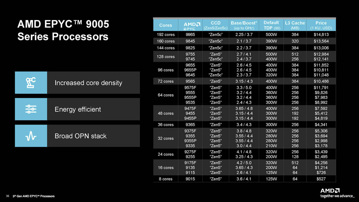
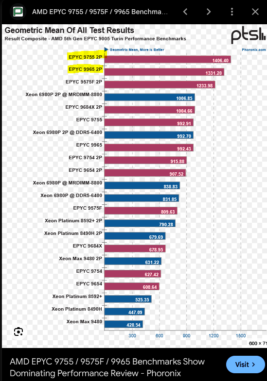
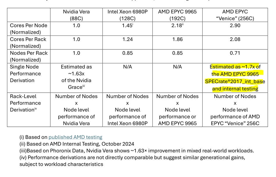
Nvidia chose the AMD 9755 even though a higher-end part and the same TDP exists (9965). Although in this scenario, higher per-thread performance is preferred over core count. So Nvidia chose the correct Turin part. Anyway, the correct comparison is a 500W Venice part.
The top end AMD Venice 9996 (256-cores) has a TDP of 600W. So need to multiply AMD performance numbers by 0.83 to make it fair.
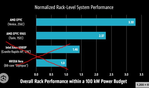
AMD has this nonsense “rack-level” marketing. Let’s compare chips. In an attempt to be fair and remove as much AMD and Nvidia bullshit as possible.
Take Nvidia Vera vs AMD Turin 9755 ratio at face value. (Phoronix Data)
Will take AMD Turin 9755 vs Turin 9965 at face value (Phoronix Data)
Will take AMD Venice 256C vs Turin 9965 at face value.
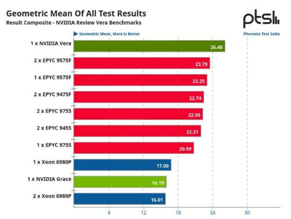
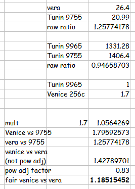
According to my shitty comic-sans spreadsheet analysis, AMD Venice is 18.5% better than Nvidia Vera.
Shame on you Nvidia for making comparisons against a 2-year old competitor.
Shame on you AMD for making some ridiculous “rack-scale” adjusted benchmark instead of just comparing the damn chips and ISO power. Your lead against Nvidia is not 3.3x, it’s 1.19x.
[6.c] Intel Dimond Rapids
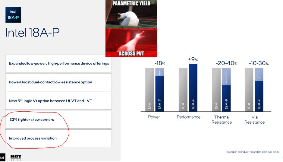
This slide is the most important one.
A Background-Proof Guide on Process Development Kits

Irrational Analysis is heavily invested in the semiconductor industry.
hint hint wink wink
Anyway let’s look at the CPU itself.
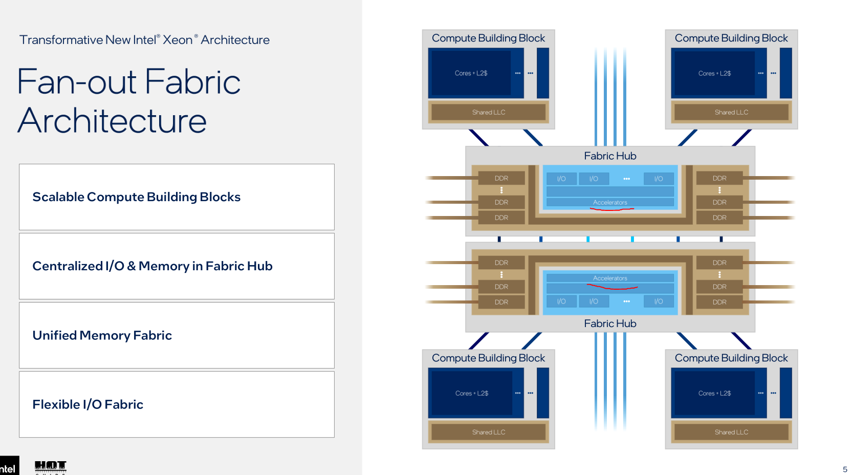
I maintain my view that most of the proprietary Intel on-CPU accelerators are bullshit and a waste of die area.
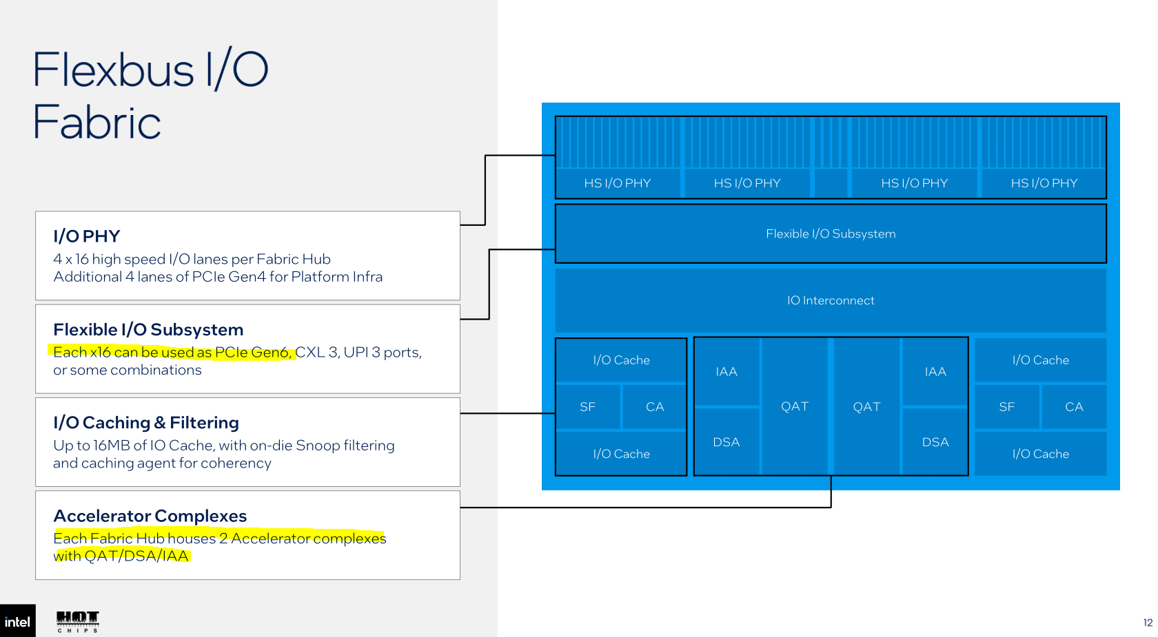
PCIe Gen6 is not high speed but whatever. I consider everything bellow 100G/lane slow.
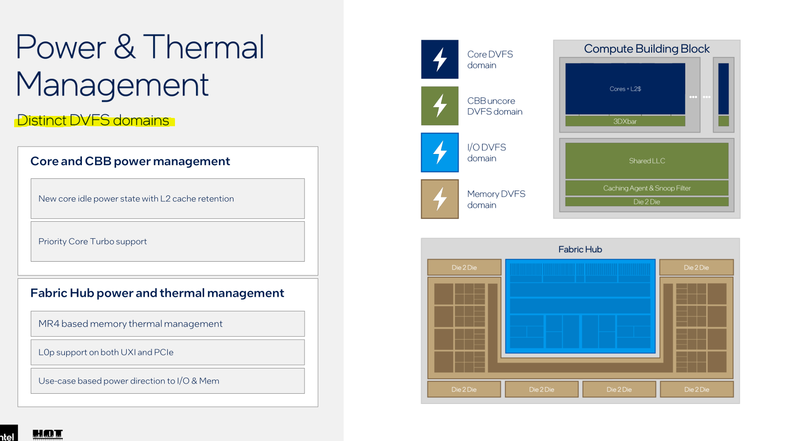
This is interesting. Adds some complexity. Curious what the power gains are for quad DVFS domain vs single domain.
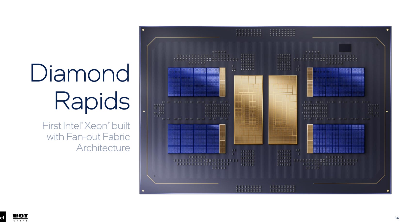
Wait wait this slide reminds me of something. One moment.
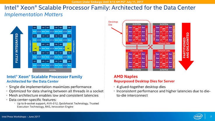
Congrats Intel! It took you 9 years but you finally figured out the optimal way to design a high-performance datacenter CPU.
*Yes I know only second gen AMD EPYC and onwards has centralized IO die. Point stands.
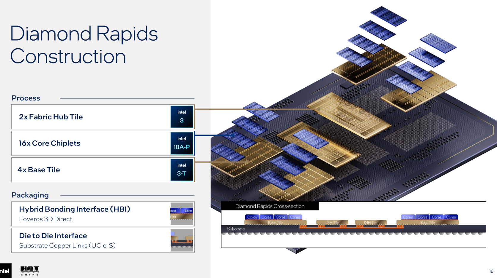
Welp now that hybrid bonding is dead from HBM de-spec trend it’s good to know the existing tool install-base has something to do. Maybe Intel can buy second-hand hybrid bonding tools from Micron.
Also good to see Intel 3 getting some use. That node is trash but the Ireland fab is tooled for it.
[6.d] ARM First-Party CPU
I despise the marketing name for this chip.
Going forward, I will refer to this product as the ARM FP (first-party) CPU because this is the first CPU they are making and selling themselves. Not an IP license. Real first-party hardware product.
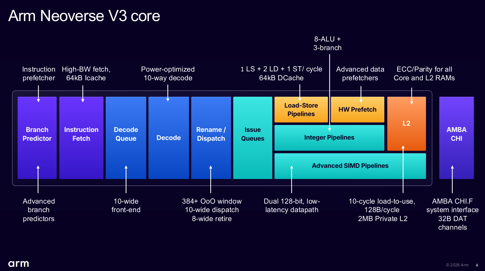
The V2 core was a disaster as previously mentioned in the Nvidia Vera section. Let’s see what is different with V3.
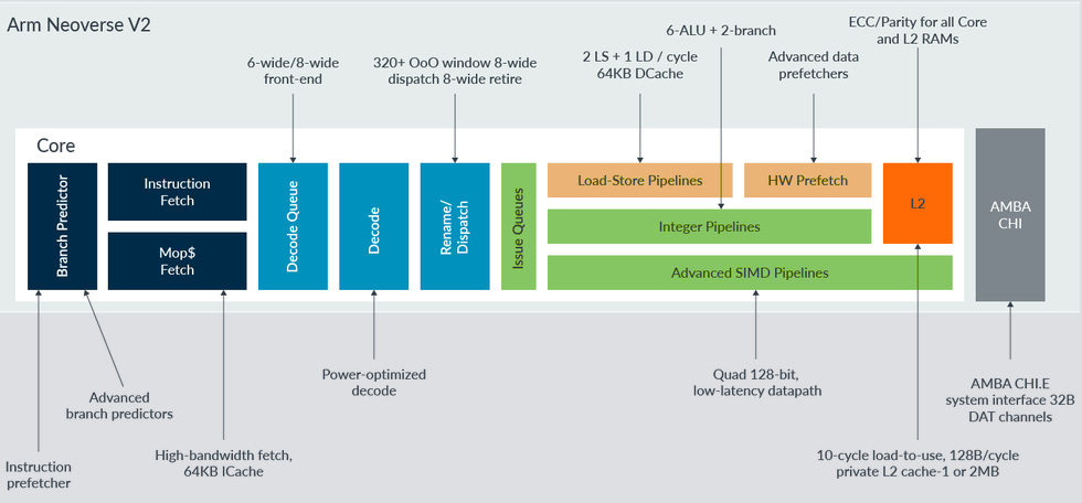
decode queue to 10 from 6/8.
OOO window raised to 384 from 320.
My understanding is the main issue with the V2 core was a buffer in the control logic (I think within the branch predictor) was way too small and would be easily saturated. Honestly don’t remember. Not a programmer so did not deal with this first-hand.
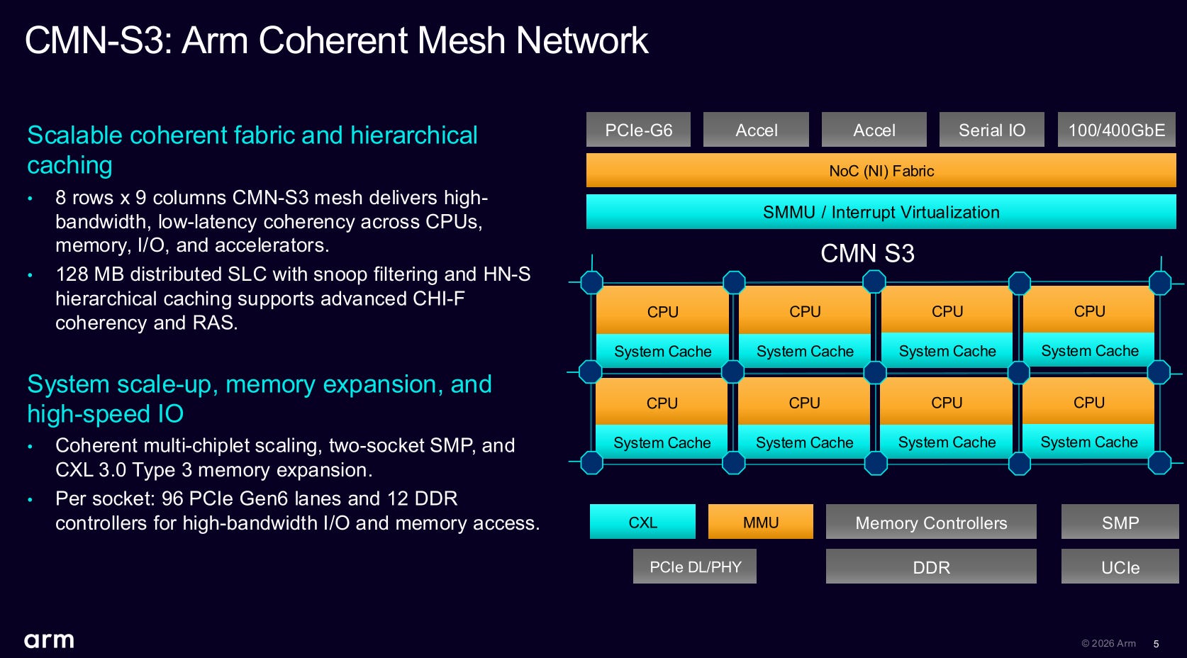
The other big problem with Nvidia Grace was Nvidia’s (very dumb) decision to not use ARM CMN and instead use a crap Mellanox-designed NoC. So in a way, Grace being garbage is both Nvidia and ARM’s fault.
CMN is very good. Only a small handful of companies have better first-party NoC IP. Nvidia is not one of them. :)
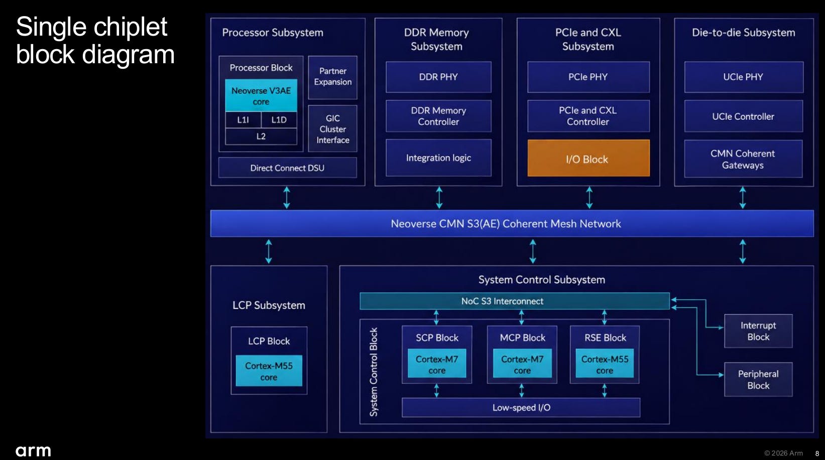
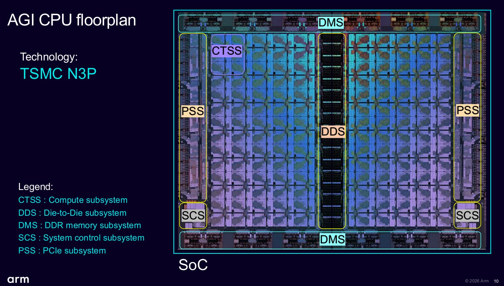
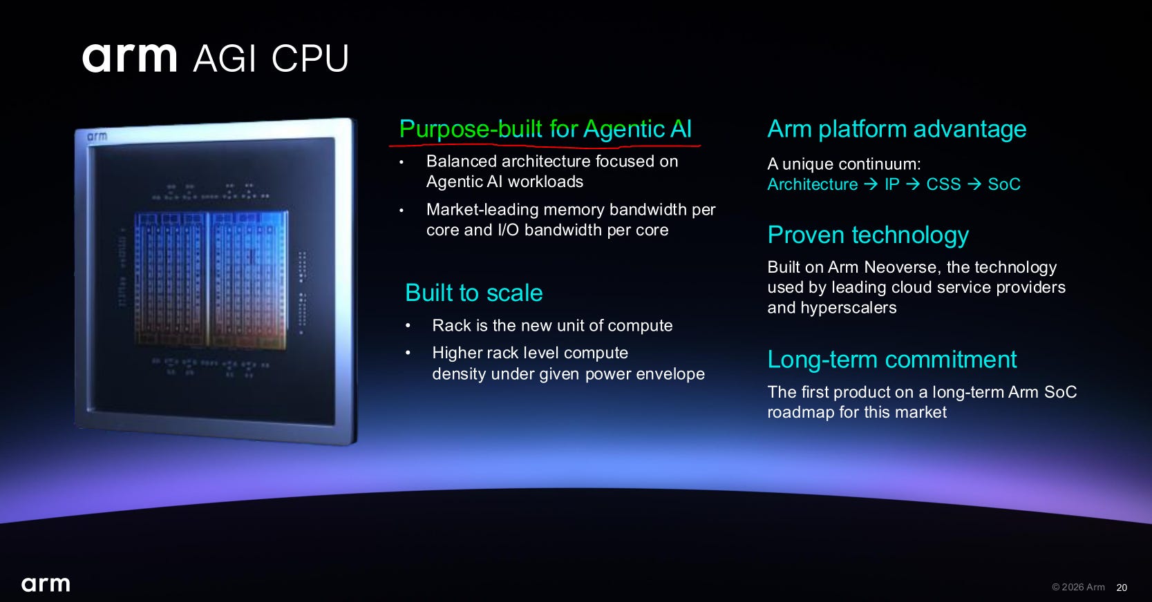
AMD Venice is going to be much better for Agentic AI. I fail to see how this product is “purpose built” for agentic AI. It’s a good all-around CPU.
[6.e] Fujitsu Monaka
Fujitsu makes custom ARM-ISA compatible CPUs for supercomputers. They are a fun group. Make interesting design decisions.
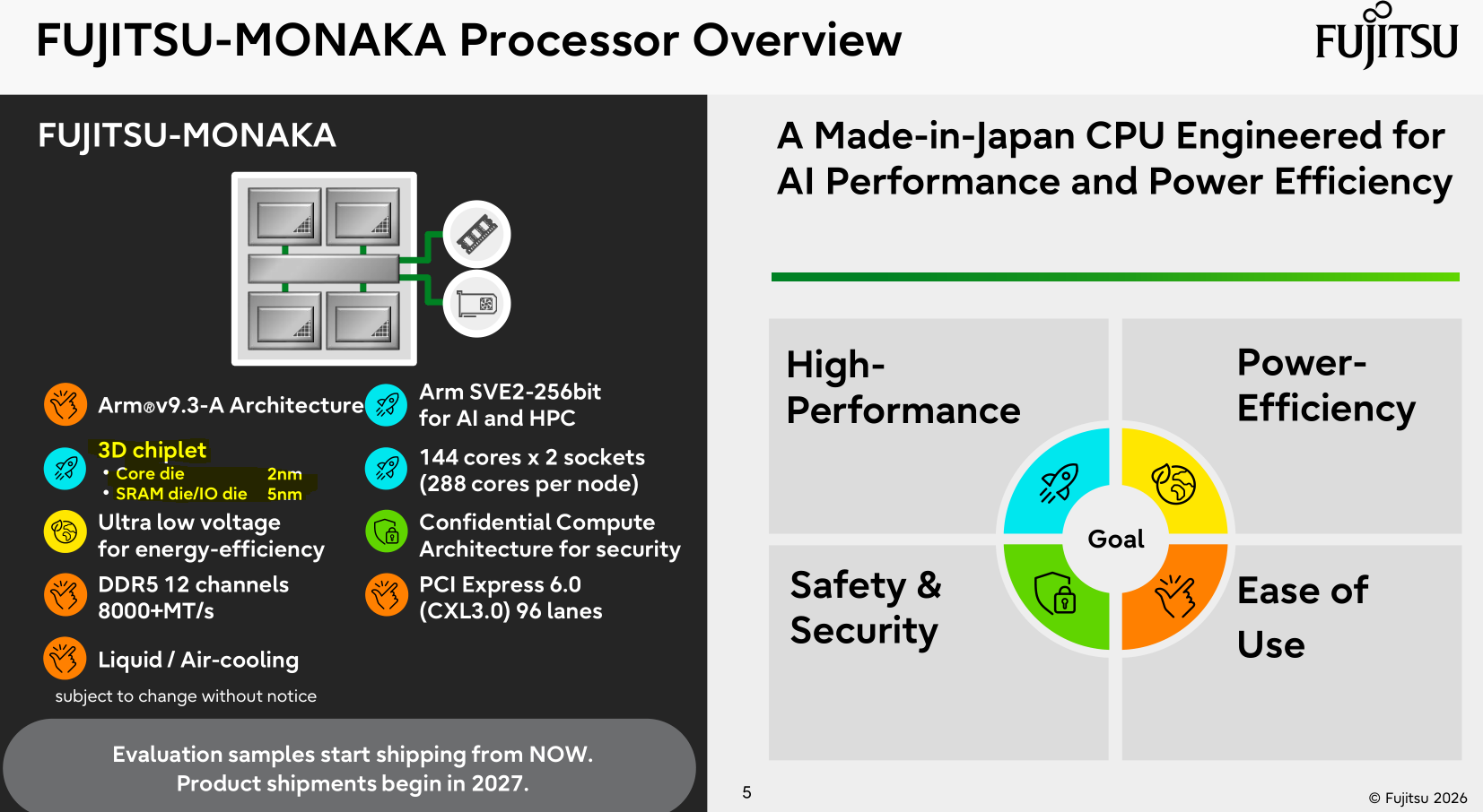
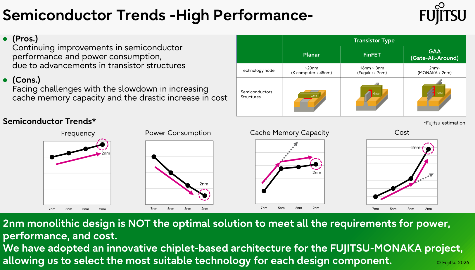
Thank you captain obvious.
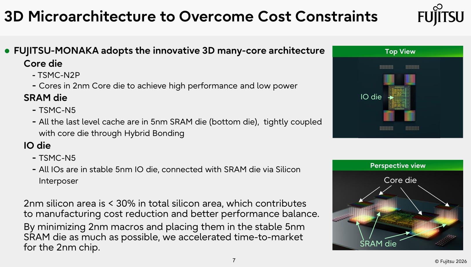
Love to see hybrid bonding now that AMD chickened out. Genoa-X was the last hybrid-bonded EPYC CPU. SAD!
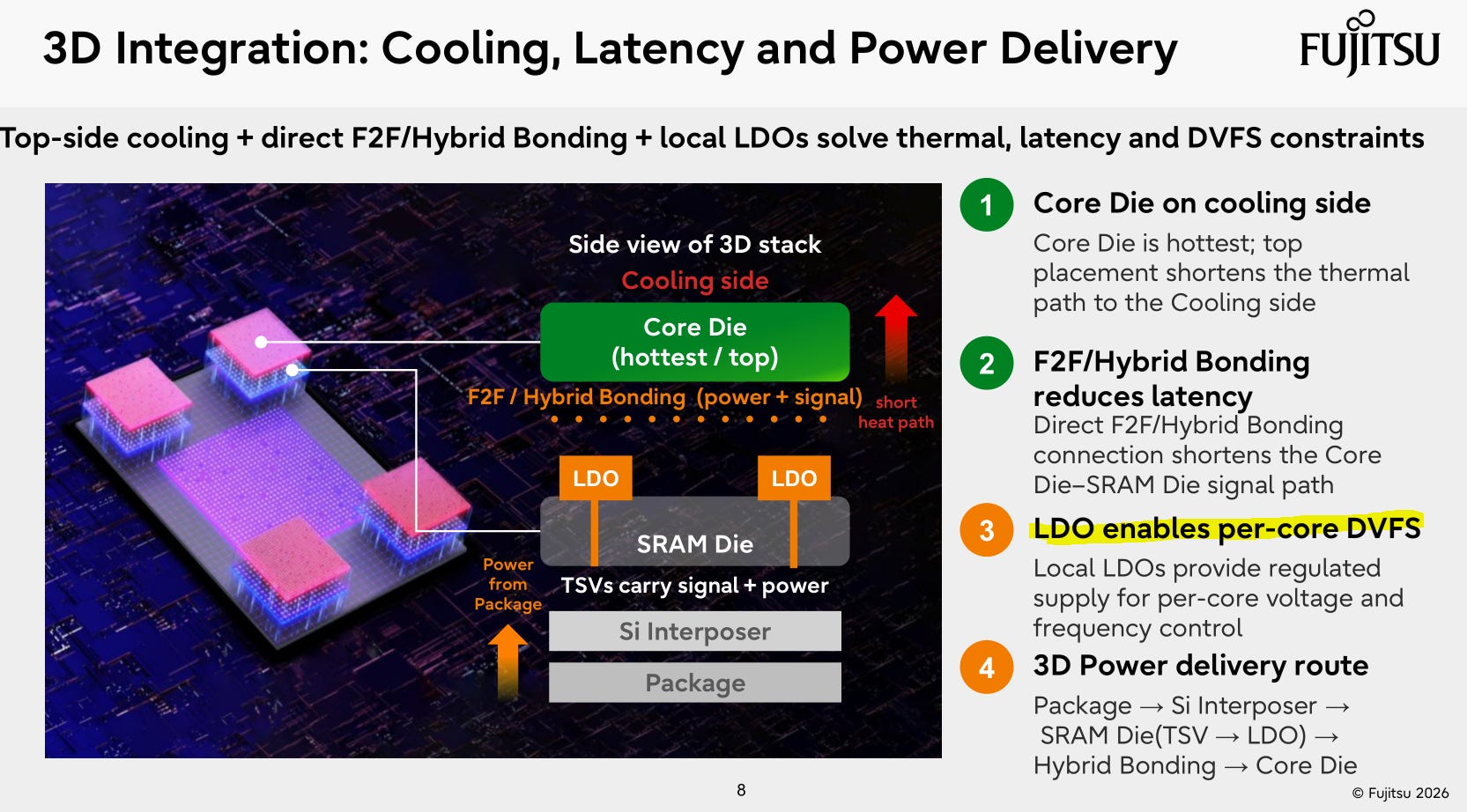
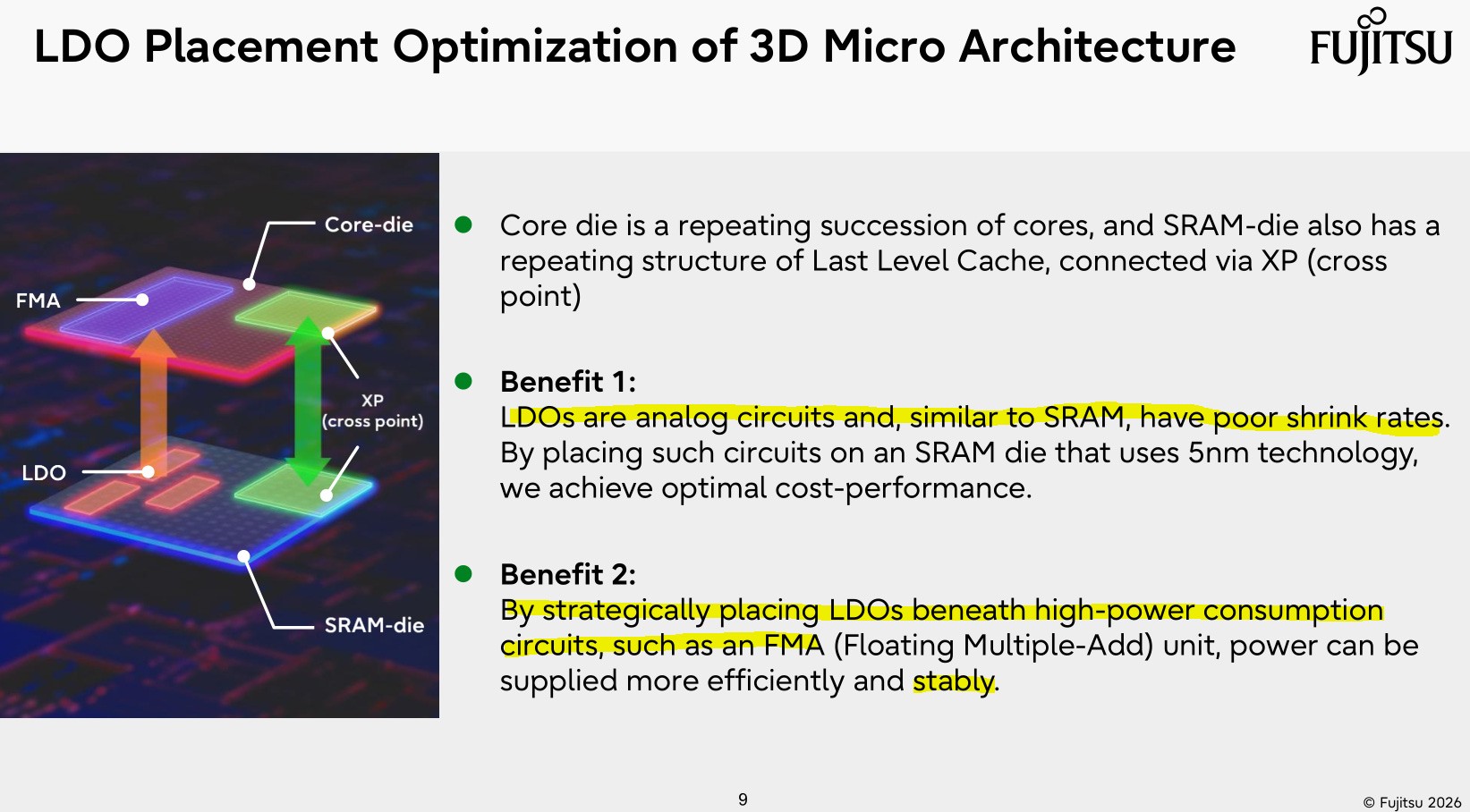
This is a nice trick. LDOs have poor efficiency but if you can undervolt each core individually (granularly) its super worth it.
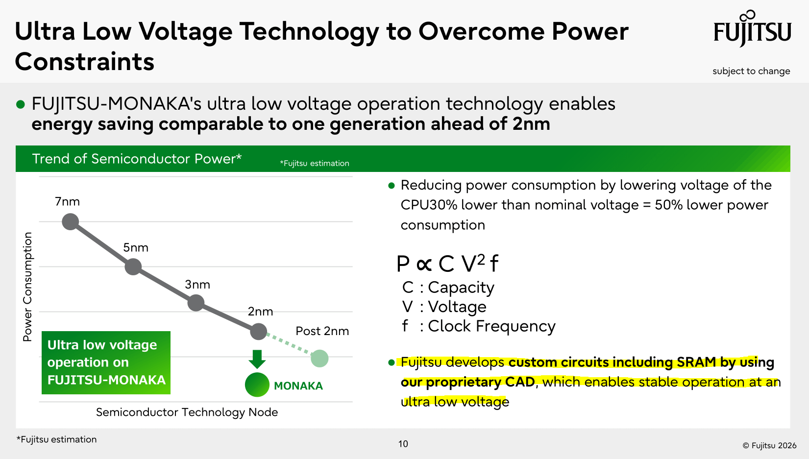
This is bullshit and Etched is also peddling this low-voltage secret sauce. Will cover in more detail later megapost.

[7] Roast of RISC-V
RISC-V had half the tutorial day dedicated to them but I want to start with this automotive talk.
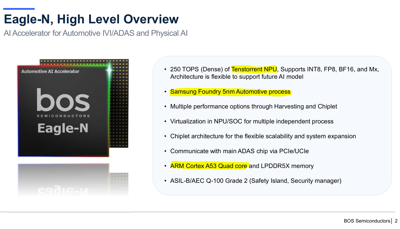
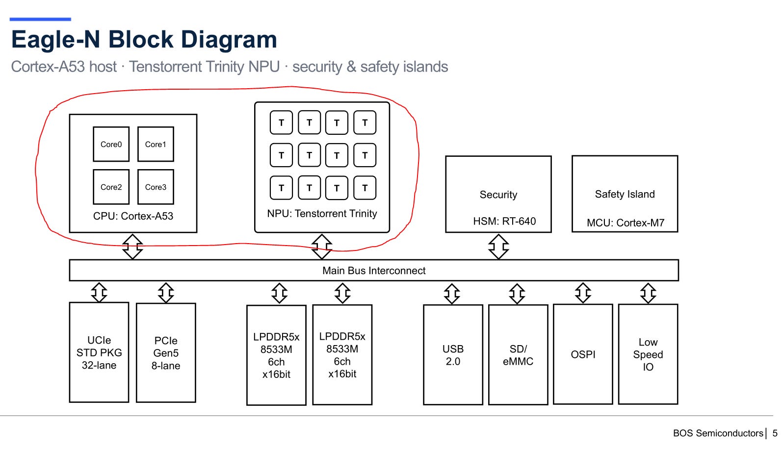
Tenstorrent is the only company that has and sells high-performance RISC-V core IP. In fact, they have a full portfolio.
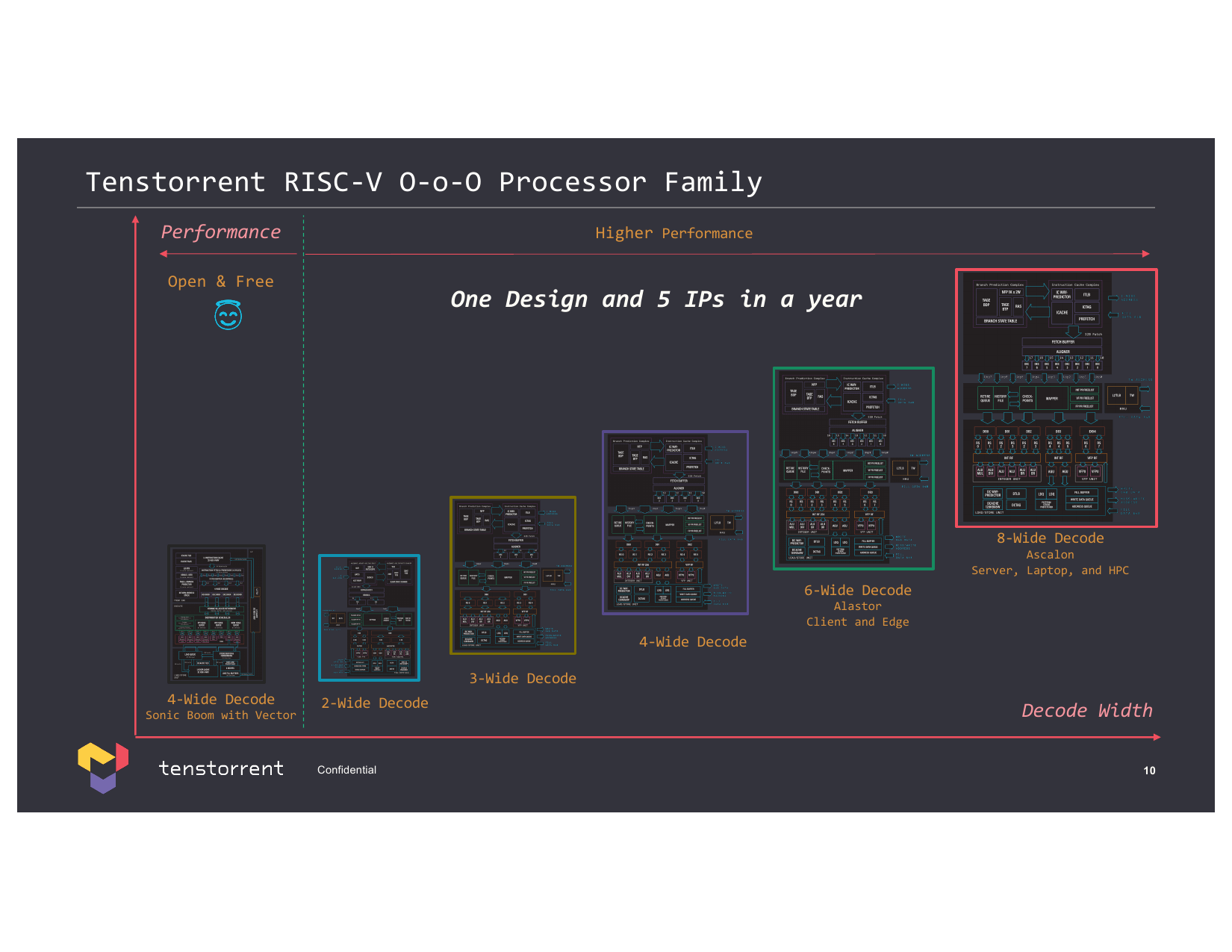
This portfolio is available on Samsung SF5A just like all their AI/ML IP.
And yet, BOS Semi chose to use the ARM A53 core, dogshit from 2014.
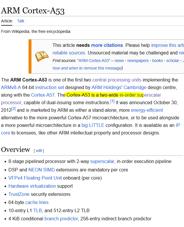
Even back in its day, the A53 was dogshit. Apple humiliated ARM and every Android SoC shop that used A53+A57. It was a disaster. In-order, two-wide.

I assure you without looking at any benchmarks that that the worst RISC-V core design IP Tenstorrent has would be at least 10x better than the ARM A53 in blended PPA.
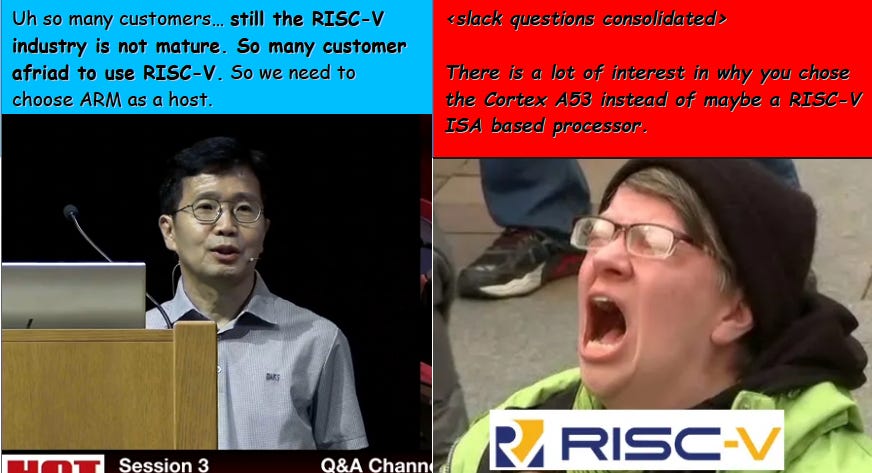
And yet despite having an existing business relationship with Tenstorrent, BOS Semi chose this utter dogshit over RISC-V. What does this tell us about RSIC-V?
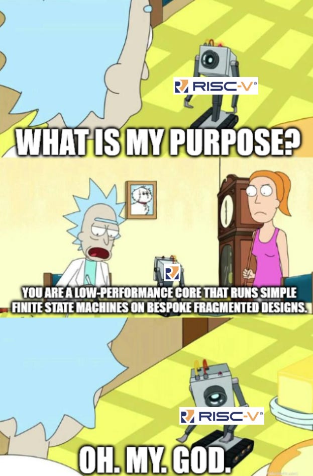
Let’s find out. The Q/A section is full of RISC-V fans who I have visually approximated to the following meme.

In the IBM talk on their dual-ISA (Z with ARM added now) CPU, again the RISC-V losers asked “why not us?!”. The response was obvious and given by the IBM presenter.
Nobody wants RISC-V. There is no business case or ecosystem.
With the introduction out of the way, let’s go over the RISC-V specific presentations.
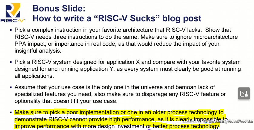
First three bullet-points are waste of time nerd cope. Going to ignore that.
Last bullet point is hilarious. Idiot who is presenting is from SiFive.
Three years ago, SiFive fired their entire datacenter team. 130 people.
Maybe the reason there are no “good” implementations on modern process technologies is because you (SiFive Chief Architect) fired the entire datacenter team three years ago.
Even the best and most competent RISC-V company (Tenstorrent) lost to the fucking A53. Maybe there is a problem with the architecture, Mr. Chief Architect?
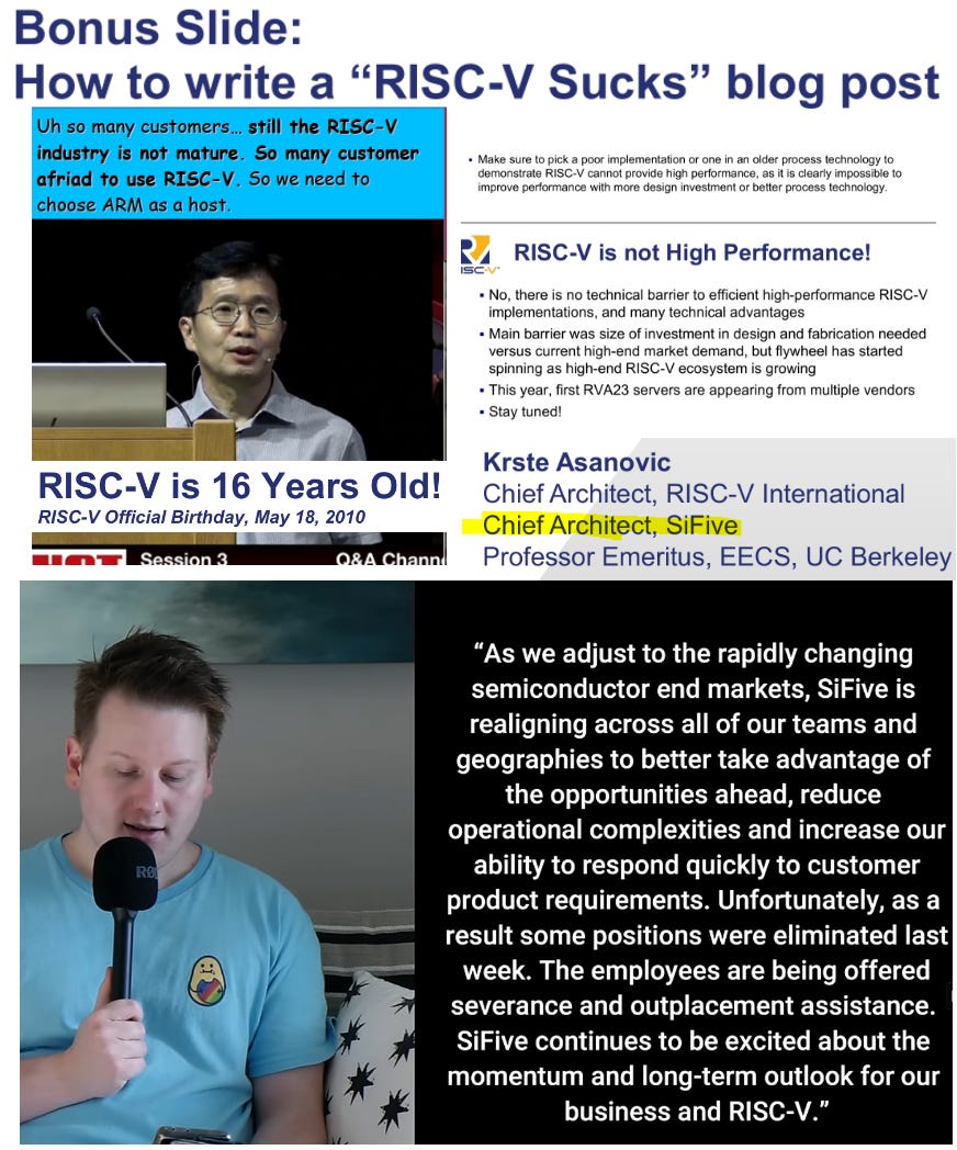
The entire presentation reeks of teenage angst. It’s genuinely funny.


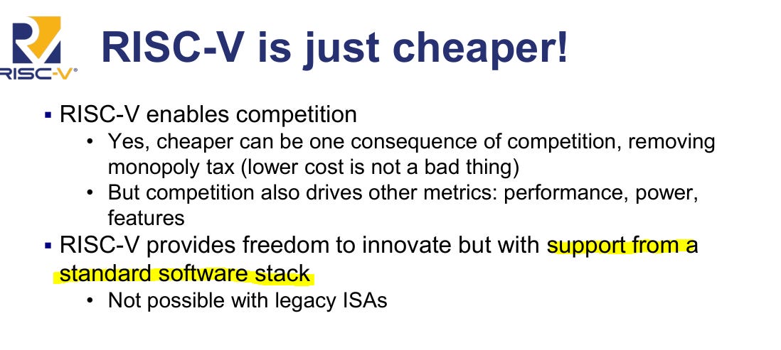
Bro what standard software stack?
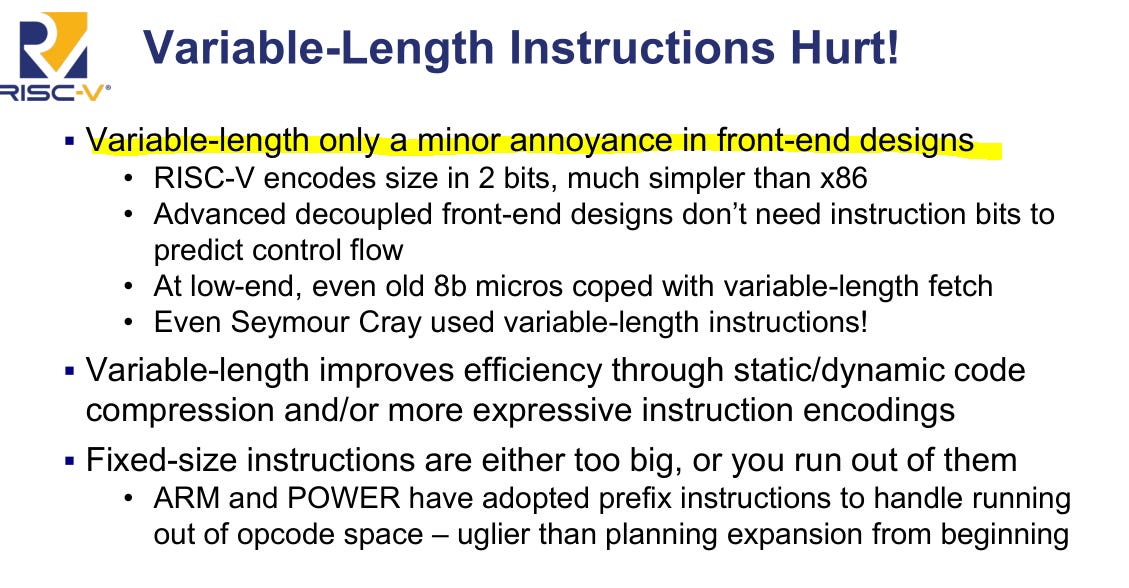
Variable-length instructions are indeed a problem. Qualcomm, the company that is frankly most incentivized to migrate away from ARM after ARM literally sued them, tried to give you feedback years ago.
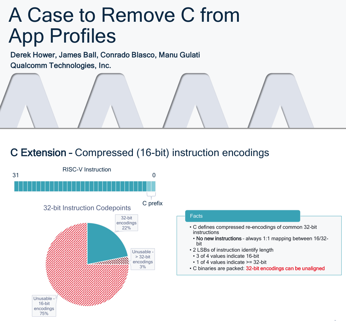
C is the name of the RISC-V compression instructions that lead to variable-length.
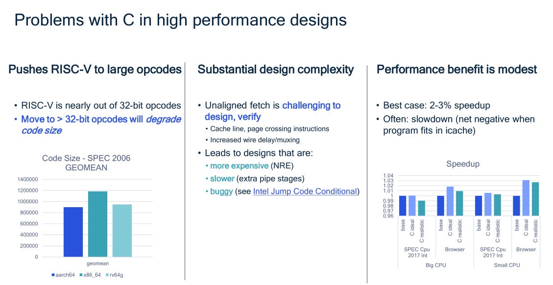
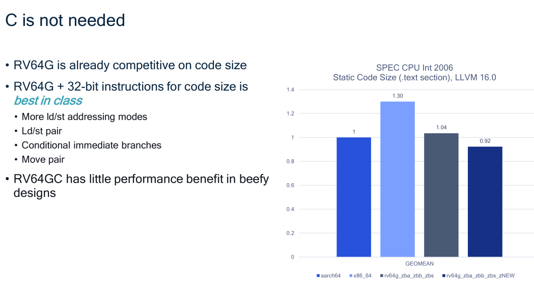
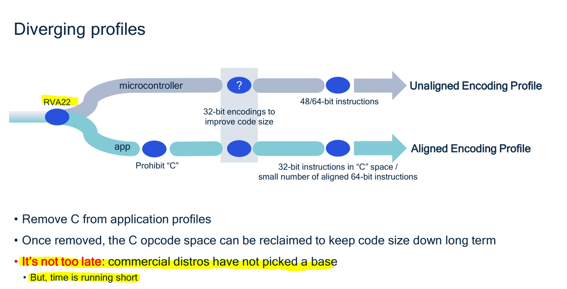
It is too late now! Whoops.
Too bad the Chief Architect of RISC-V failed to listen to technical feedback from one of the largest ecosystem players on variable-length instructions and is defending this idiotic decision three years later while wondering why nobody wants to use RISC-V.
How much annual processer revenue does Qualcomm have versus SiFive? Who knows more about ecosystems and commercialization?
It’s almost as if RISC-V is a clown show standards body.
In various dayjobs, I have had to interact with standards material (IEEE 802.3, OIF, 3GPP). It’s rare when member company presentations add bold red text to their presentations lmao. Honestly I think this is the first time I have seen such aggressive posturing within standards meeting slides.
Next up is Ubuntu.
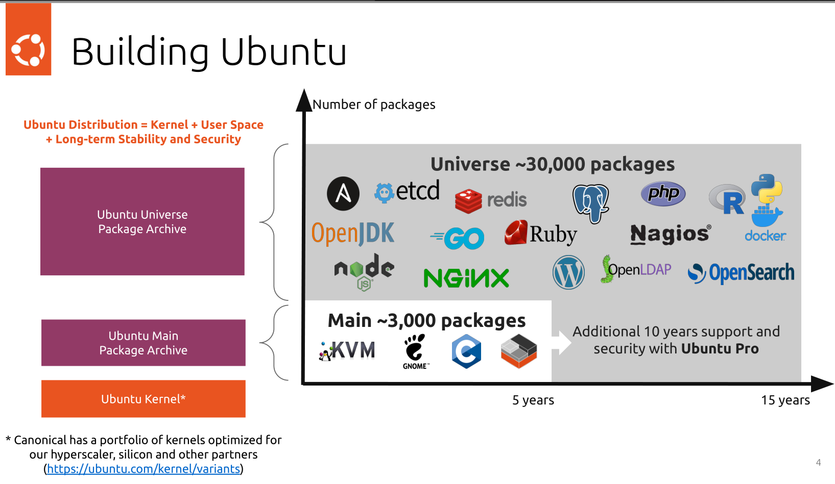
Ubuntu is a shitty derivative of Debian.
If you want to install and use Linux, just use Debian or some other lightweight Debian-based distro such as MX or Mint.
Canonical is incompetent and adds so much crap to Debian. Best example is Snaps. They made their own shitty proprietary package manager which conflicts with APT.
All right Nvidia what u got for us in the RISC-V section?
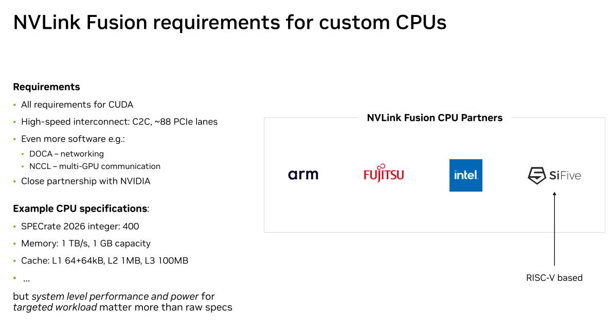
Yes SiFive is going to sweep in and made a datacenter-class CPU for NVLink fusion. 🤡
Tenstorrent could pull this off but Jim Keller is too busy coping over Ethernet.

[8] Miscellaneous
Various topics that don’t fit a particular theme. Some of these are summaries of organic conversations with interesting people.

[8.a] AMD/Xilinx RF FPGA
In a previous life I worked on wireless. These FPGAs are super cool but economically useless. Dead industry.
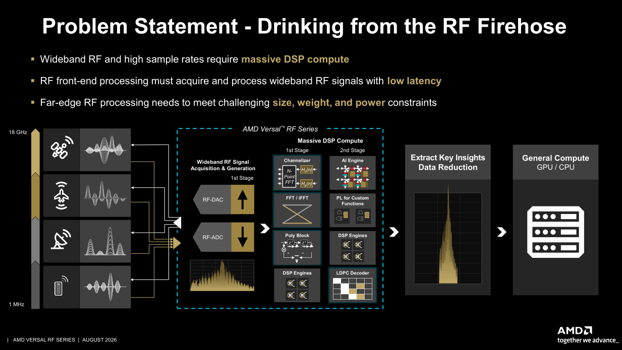
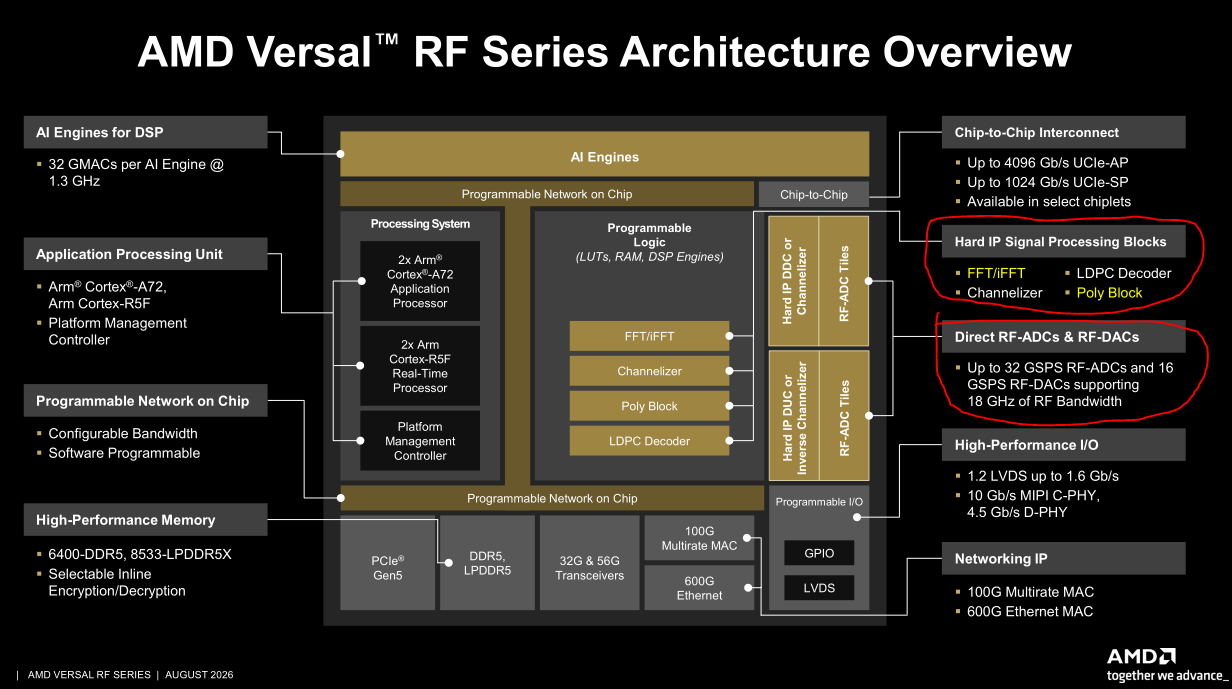
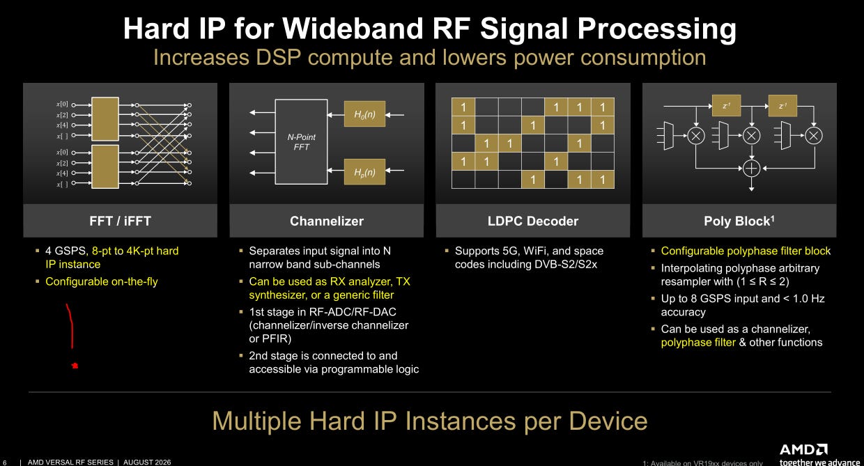
THIS IS SO COOL. 99% of you have no idea what these words mean but its legit incredible hard-IP acceleration blocks for real-time DSP.
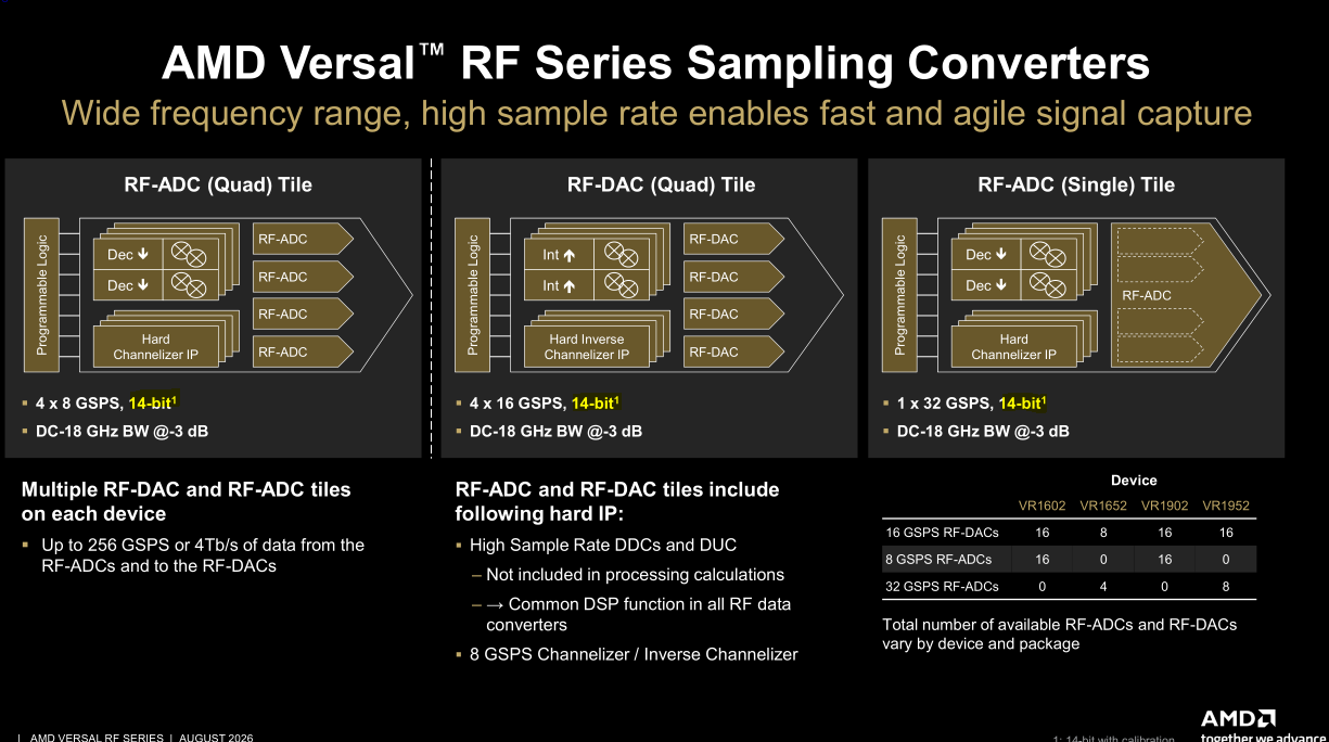
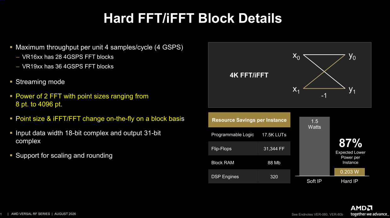
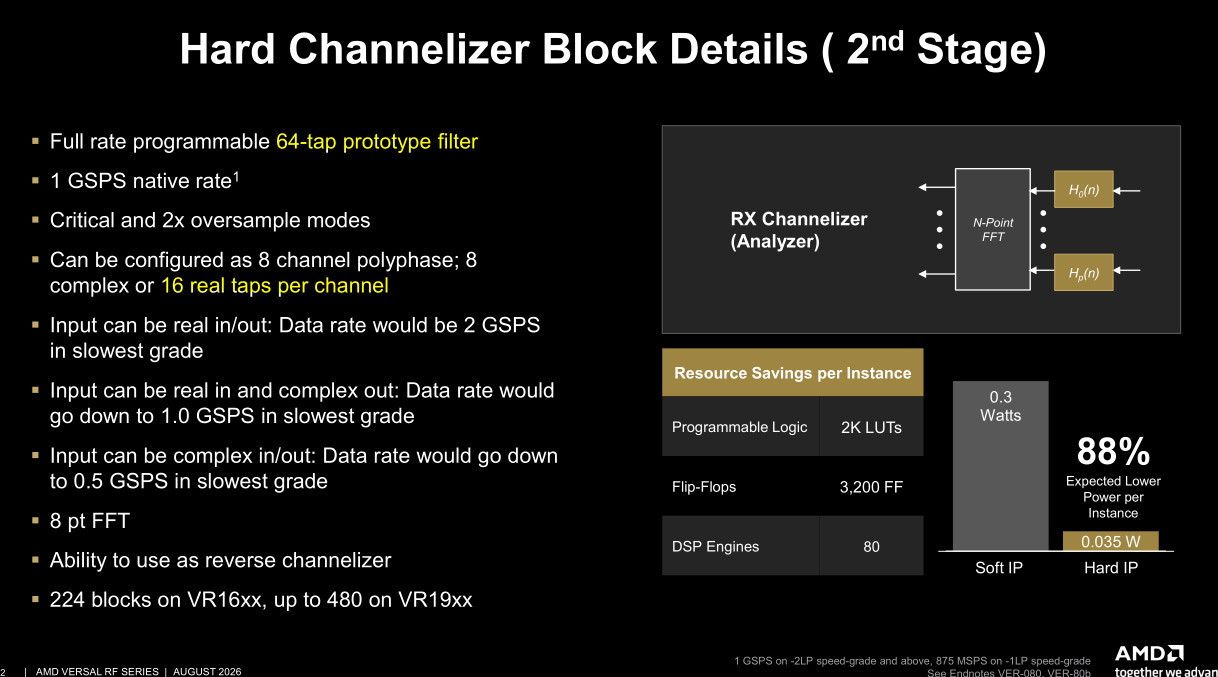
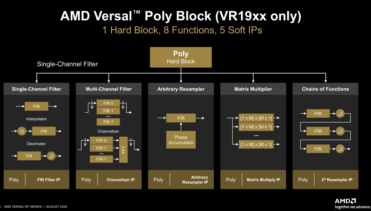
The amount of flexibility this FPGA enables is astounding. The filtering options are so fucking good.
[8.b] Opticore
Note: A private copy of this section was shared with Opticore so that they can debate technical matters. Also visited their lab. Credit to their CEO (Zaijun) for taking the time to answer questions in front of a whiteboard at great technical depth and honesty.
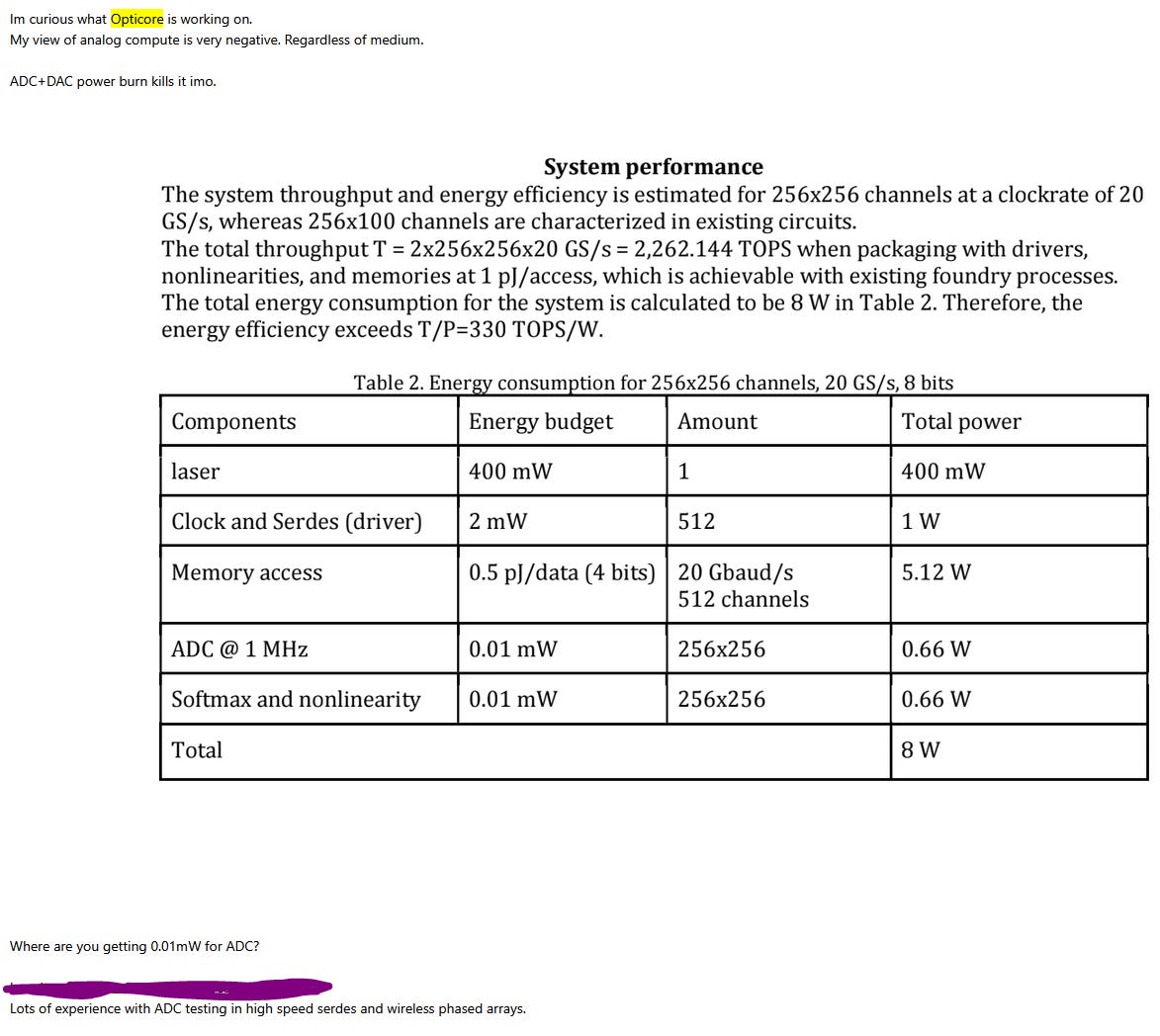
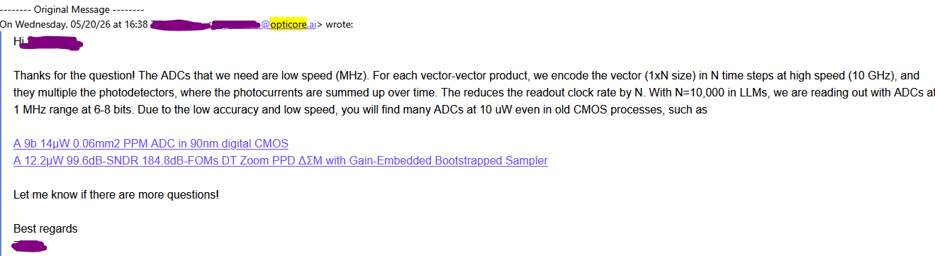
I generally dislike all forms of analog compute regardless of the medium. Optical, thermal, resistive, and so on for two reasons.
1. DAC+ADC power burn invalidates the power saving claims.
2. Out-scaling CMOS digital logic in an economic way is basically impossible.
In a previous conversation, Opticore gave an excellent answer for #1.
After visiting their office and discussing their strategy at length with Zaijun (CEO) I am willing to set aside problem #2 as theoretically solvable. At least to the point where Opticore can find some economic success. Their system has very interesting scaling properties.
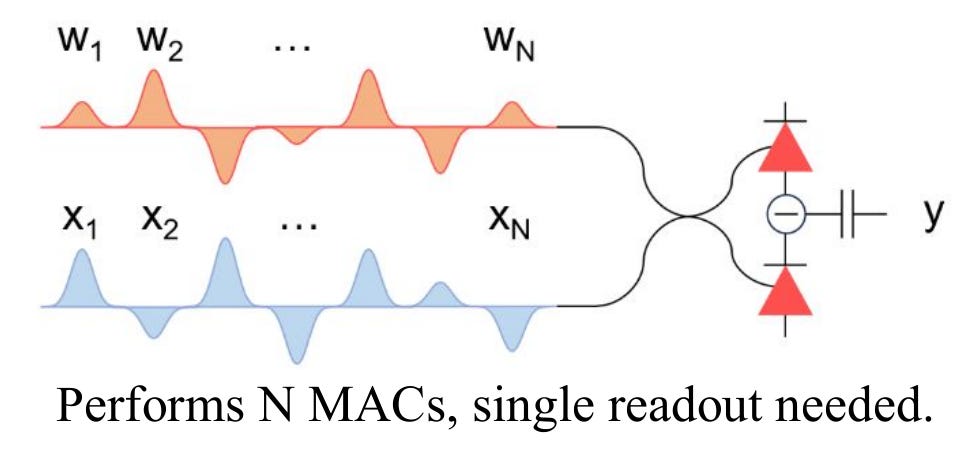
The core trick is preforming MACs using balanced photodiodes. Usually BPDs are in coherent transceivers as they cancel correlated noise very well.
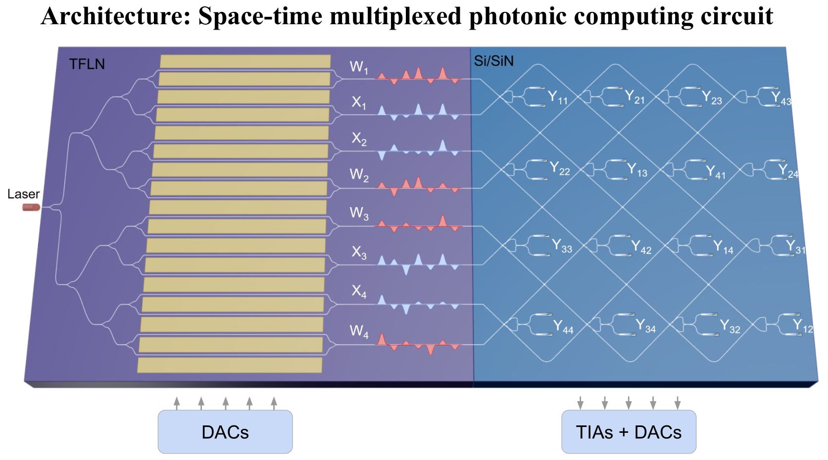
TFLN modulators are used to encode data into the CW laser light. Going forward, Opticore will be using ring modulators because they want to maximize channel density and TFLN modulators are simply too big to scale.
This is great because I hate TFLN. It’s a joke meme PhD material that cannot be manufactured economically at scale.
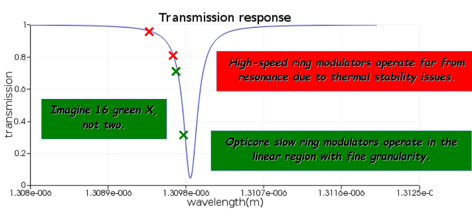
Rings are very unstable but Opticore is only using one wavelength from a single laser. Thus, the normal thermal crosstalk issues of DWDM laser drift don’t apply. Instead of using a PID loop for each ring, thermals are stabilized with a simple PLL.
Each ring is also running so slow, Opticore can run them more aggressively, achieving higher extinction ratio and thus more margin for PAM16 encoding. I was very surprised by this. Only Nvidia has done PAM4 at high-speed on ring modulators. Ayar Labs and Lightmatter both are making claims but have no public data to back it up. Apparently at low speed, researchers have done up to PAM64. It is much easier to operate rings in the linear region precisely at low speed.
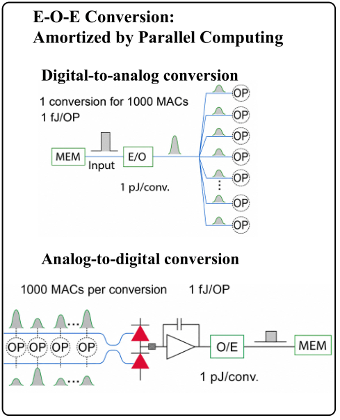
The most important aspect of any analog compute effort is dealing with DAC and ADC power burn. Opticore has a very good story here. I was going to torch them over this but they have done a great job.
They also have excellent calibration results.
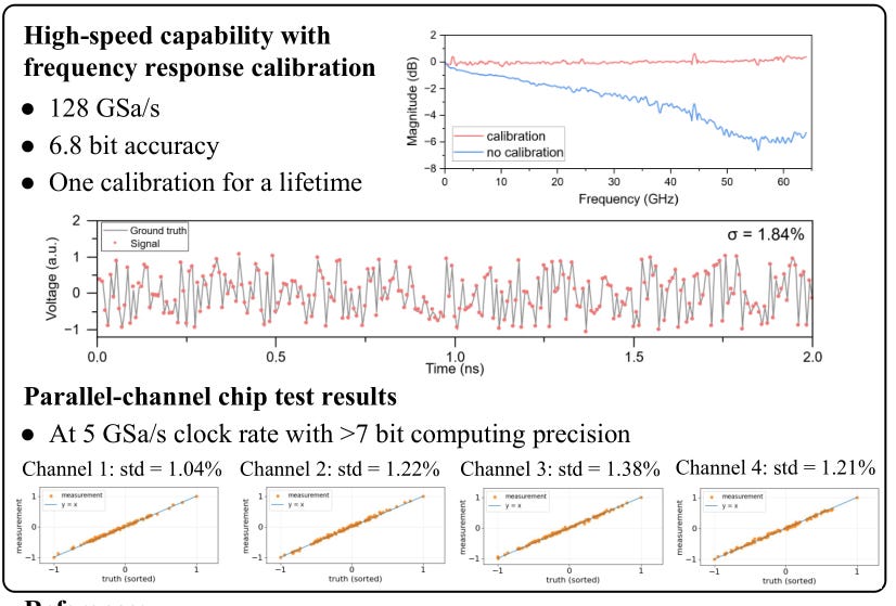
I have had to deal with DAC and ADC calibration (DNL/INL) across several dayjobs. These charts are kickass. Very well done. Still, electrical crosstalk will be an issue but at least per-channel calibration has been dealt with.
Finally, there is the question of reliability. In traditional SiPho systems such as transceivers, the PIC is wire-bonded. Reliability of photodiodes is a real and very annoying problem. Yield issues from dead PDs or degraded PDs is a real problem.
Was initially very aggressive towards Opticore on this front. Normal SiPho chips have maybe 5-20 PDs for data conversion and internal chip monitoring. Opticore has… way more and as they scale they gona have crazy number of PDs.

Zaijun claims they have 10 test wafers (each with 40-50 dice) and not a single PD on any of their chips has failed. After going back and forth on "ok great why… how is this possible” we concluded that Opticore greatly benefits from not having to use wire-bonding.
Wirebonding involves significant heat and pressure applied to pads on the SiPho chip. There are also lots of ESD opportunities. Opiticore uses face-to-face packaging with their EIC. This is a credible explanation for why Opticore has had zero PD failures so far.
This company is super interesting, I wish them well, and looking forward to updates.
[8.c] Chat with Ashkan (Photonics God at AMS OSRAM) on VCSEL CPO/NPO
Note: A private copy of this section was shared with Ashkan for feedback. No opinions were changed. Mainly needed to check technical correctness and if certain details were ok to publish.
I managed to catch up with Ashkan during a break and discuss micro-VCSEL based advanced optics (CPO/NPO).
Shared with him my theory that AMS OSRAM’s competitive advantage in this space over giants such as Broadcom, Lumentum, and Coherent is their background in LEDs and dense packaging. Bluntly, the overall quality of AMS OSRAM VCSELs (WPE, output power, drive requirements, chirp, RIN, … ) is going to be worse that the much larger competitors (AVGO/LITE/COHR) who have far more experience with VCSEL tech.
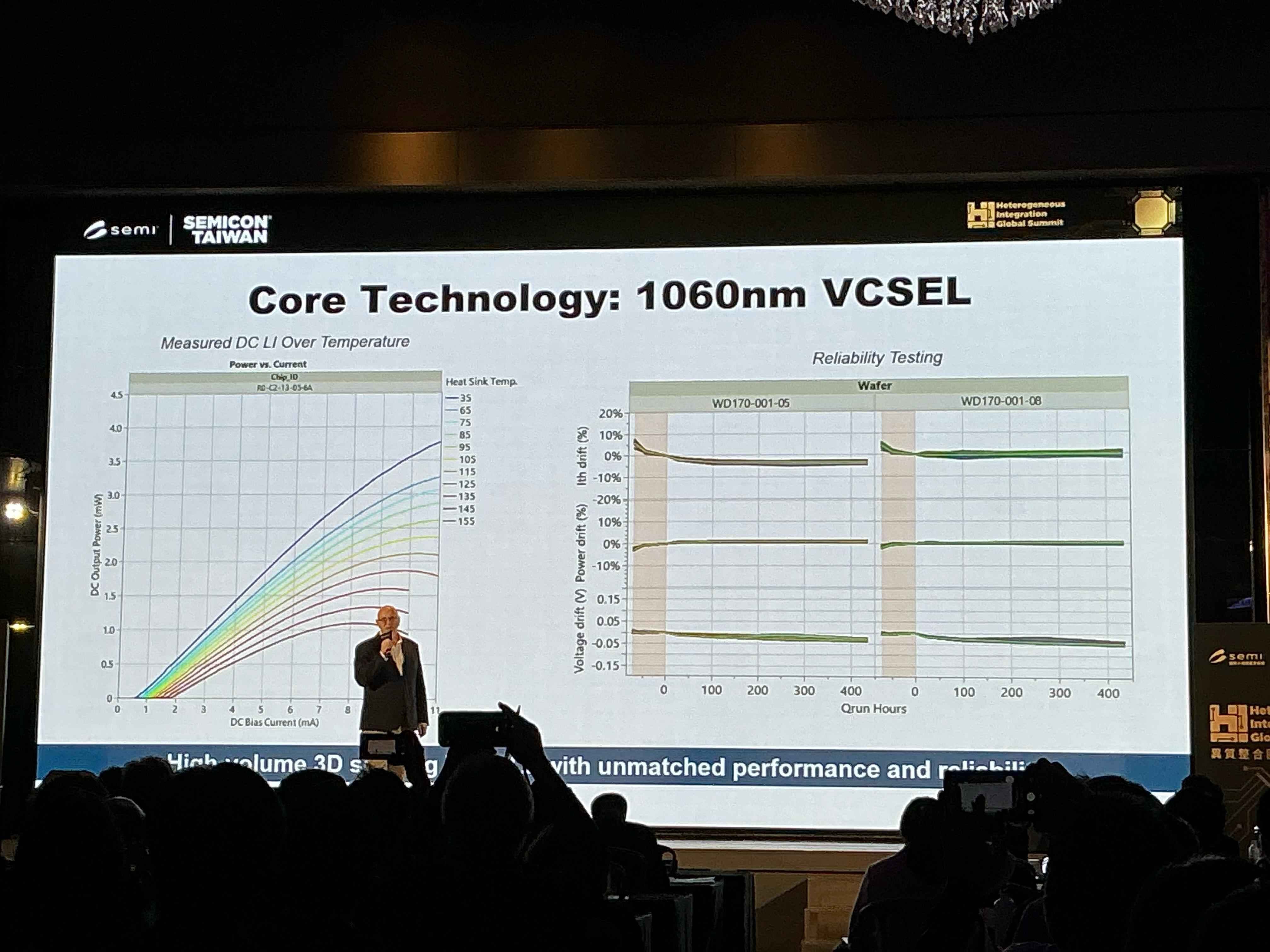
However, the quality of the VCSEL is frankly not that important for NPO/CPO applications. The goal is slow-and-wide over < 30m of fiber.
AMS OSRAM has experience and differentiation in stuff that does matter for NPO/CPO.
Dense packaging experience from LED business.
Wafer-to-wafer bonding of compound materials (AlGaAs, GaAs, InGaAs) to TSV based CMOS interposers/backplanes. Again levered from the LED business.
Dense fiber array attach at high yield.
There is also the question of wavelength.
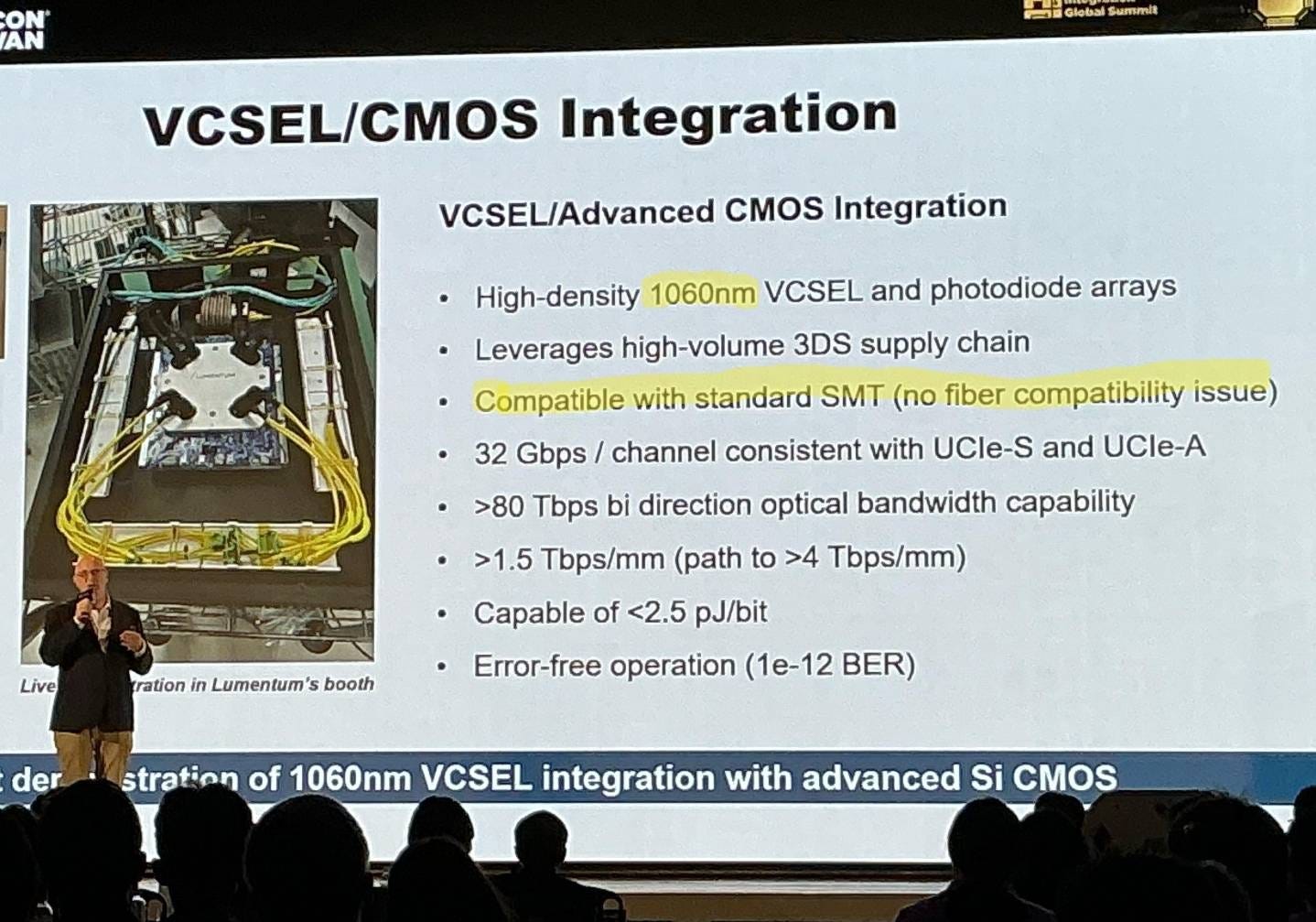
Lumentum and Coherent are both moving from the traditional 850 nm wavelength to 1060 nm. The reason why is interesting.
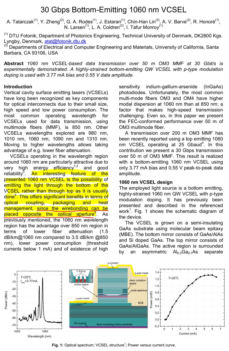
In order to optimally and densely pack many VCSELs together, you want to emit light from the bottom rather than the top. This runs into the obvious problem of having the substrate block the light. They key feature of 1060 nm light is it shoots right through standard substrate materials. The problem is in the fibers.
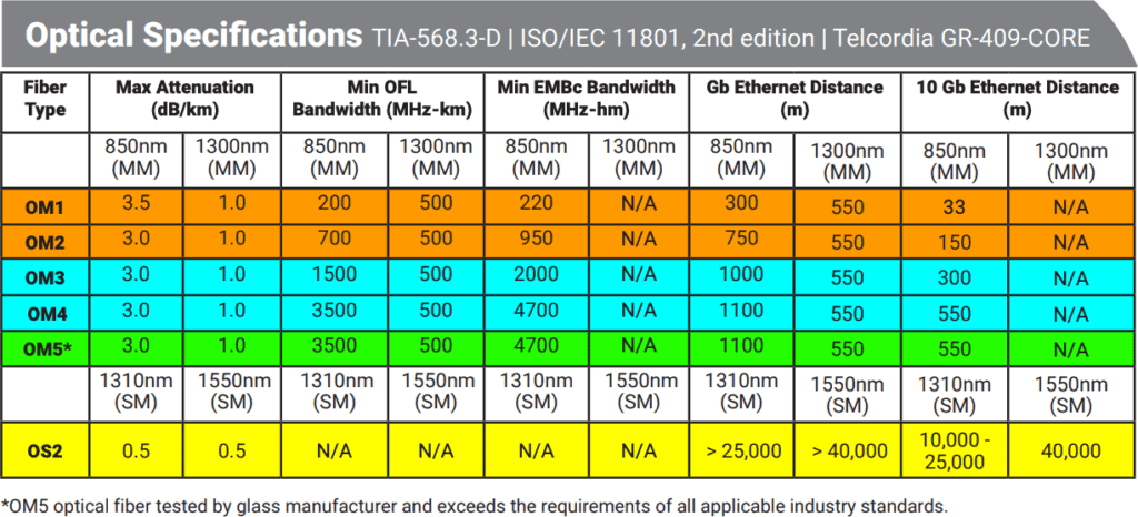
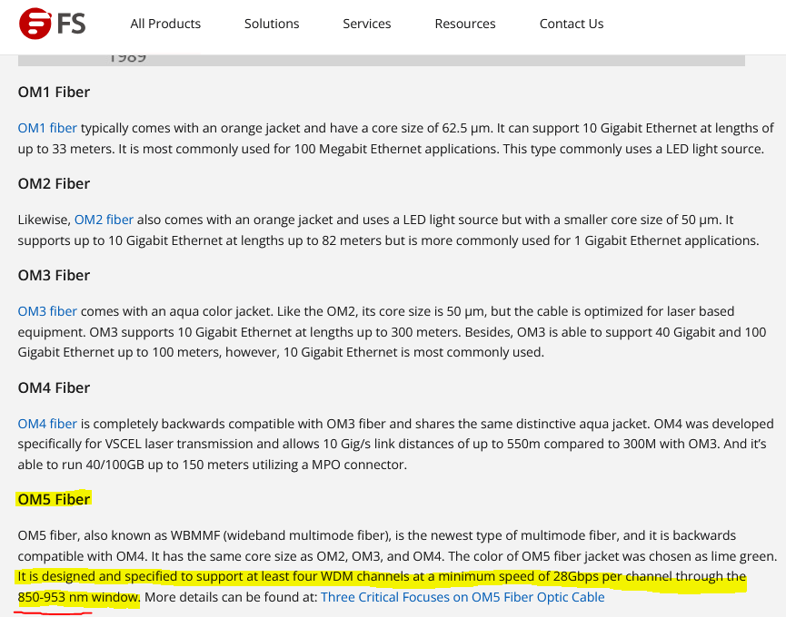
Standard OM (optical multimode) fibers are not designed for 1060 nm light. This leads to… annoying problems.
Nobody measures their fibers at 1060nm so there is no data on attenuation or chromatic dispersion properties.
Manufacturing variation of existing OM fiber suppliers is a real risk because… nobody has ever bothered to control their fabrication process at 1060nm. Literally not a single public datasheet has info on 1060nm operation. Batch to batch variation from a single supplier is likely.
To compensate for OM fiber variation/problems at 1060nm, the rest of the system needs to be over-designed. Usually the driver and TIA. Harms energy efficiency.
It is possible to measure, quantify, and control the quality of OM fiber at 1060nm but this is annoying and will slow Lumentum and Coherent down somewhat. Solvable nuisance.
Finally, 1060nm VCSEL needs a new material while normal 850nm VCSEL is AlGaAs which has already passed GR-468 reliability testing MANY times over the last 40 years.
Lumentum and Coherent both need to qualify their 1060nm VCSELS at both a device and system level according to GR-468. This is a 6-12 month process. Optics reliability testing is hell. HTOL is 5K hours.
AMS OSRAM’s strategy is to stay at 850 nm, do the packaging well (their secret sauce) and use cheap OM3 fibers. Everyone else going to 1060 nm has to figure out this fiber problem.
[8.d] Chat with Stevan, President of Olix, on pure SRAM machines.
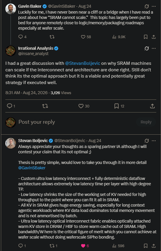
One of the great things about conferences is people are in-town and you get to have really cool conversations in-person. Stevan shared so cool info on Olix and what they are doing with 3D VCSEL scale-up that I can’t share. In truth, that was maybe 10-20% of the 2-hour whiteboard conversation. Vast majority of the time was Stevan arguing against one of my core beliefs.
For a long time, I have held the view that pure-SRAM systems are stupid and imbalanced. My mental model has been that KV cache and model weights compete with the same scarce resource (SRAM) and not having a way to offload KV to something (really anything) cheaper than SRAM is madness.
Stevan managed to convince me otherwise. It took 90+ minutes, a lot of plots, and MANY follow-up questions where I tried to poke holes in his arguments but… pure SRAM machines are fine if executed well. Still don’t think this is the optimal strategy (engineering is about tradeoffs) but willing to soften my prior (very negative) views.
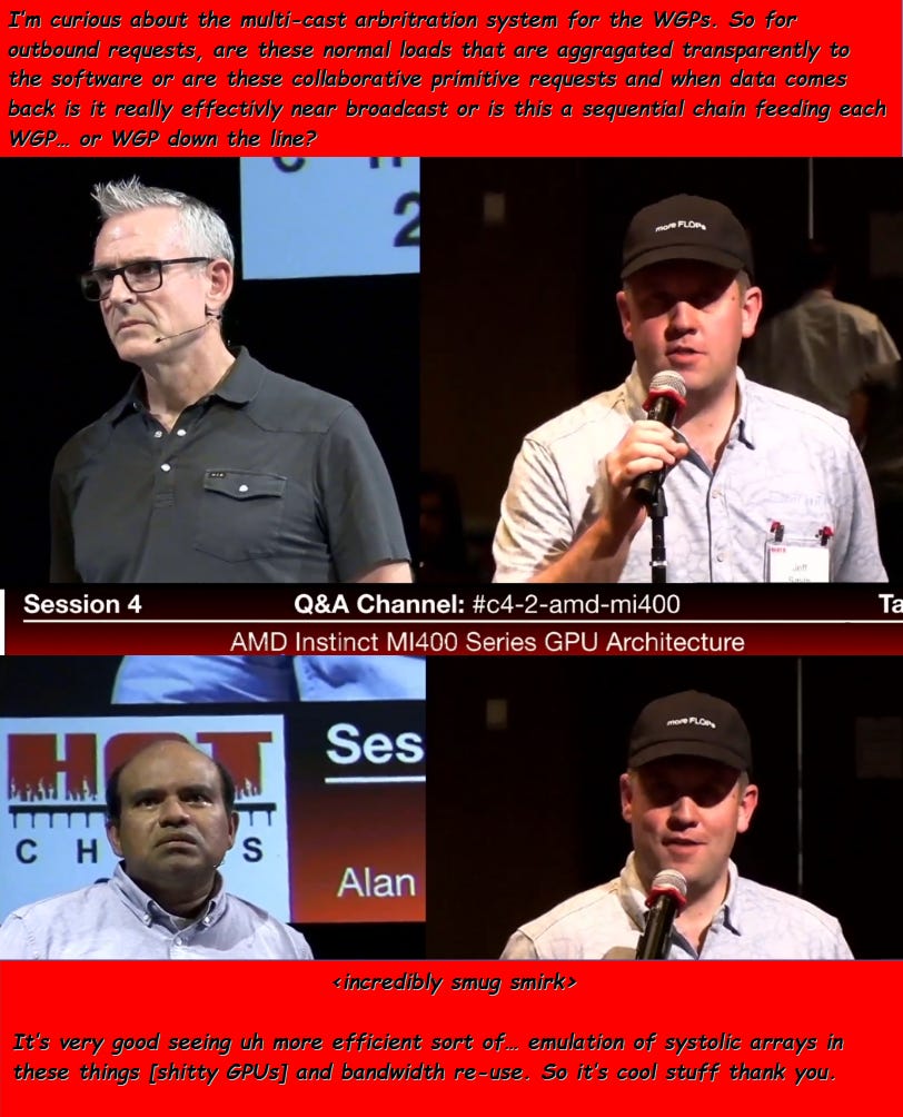
[8.e] The legend of Jeff from Etched.
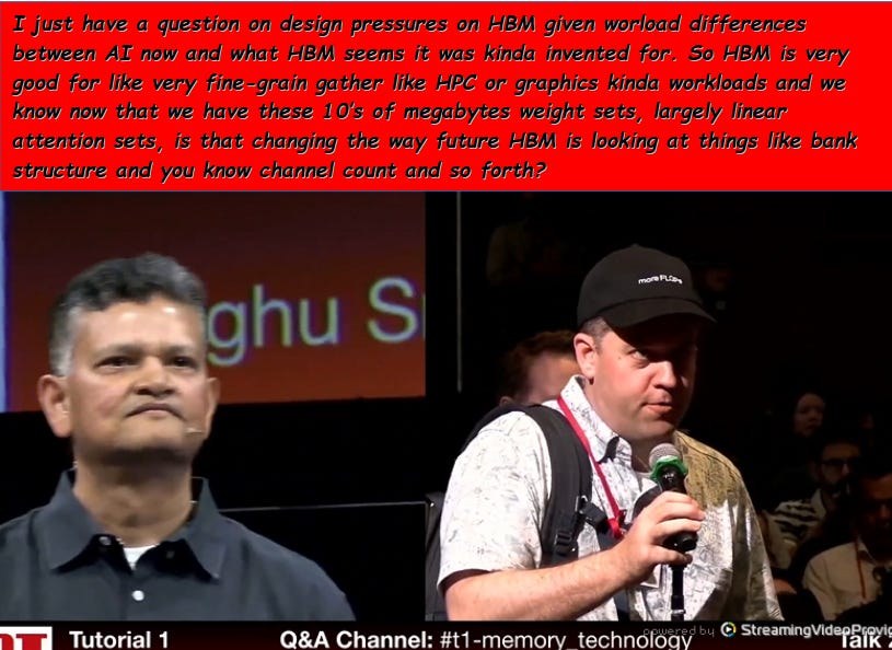
A particularly spicy person was at Hot Chips 2026. Actually he attended last year too, but with his old affiliation of Citadel.
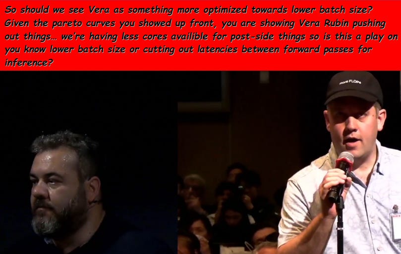
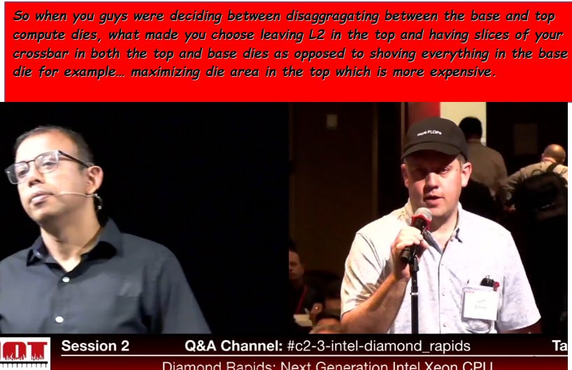
Meet Jeff from Etched. This guy showed up to what felt like every Q/A session and asked a question with the following attributes:
Excellent technical-depth.
Subtly condescending towards the presenter.
A smug facial expression and tone that makes me think “pod monkey wearing a monocle”.
I love him. Here are some highlights of this legendary hero.

[9] Higher-Level Takeaways
I want to disaggregate (pun indented) some higher-level trends and takeaways. Most of this content was in prior sections but was cut and moved here to improve flow. Well… attempt to improve flow and writing coherence.

[9.a] Multi-Vendor Disagg Inference Is Temporary
This is a spicy take that will probably piss off a lot of people but I think multi-vendor disagg inference is a temporary phenomenon.
As a reminder, I believe only four compute design entities economically matter.
Nvidia
Google/TPU
Amazon/Trainium
AMD
A small army of startups (and recently IPO former-startup) are trying to become decode disagg parasites on top of one or more of the above entities, typically Nvidia.
I want everyone to stop and think a moment about what Mr. Leather Jacket accomplished by panic-buying Groq on the last week of December 2025.
It took Nvidia+Groq only 8 months to take an existing dogshit half-broken LPU chip built on Samsung SF4X (I am well-informed on this process node and the clusterfuck that original chip was) and made a real rack-scale disagg product to compliment Rubin. Not Rubin Ultra, regular Rubin.
And the result is not bad. You can cope all you want, AI ASIC startups and Cerebras, LPU+Rubin is decent.
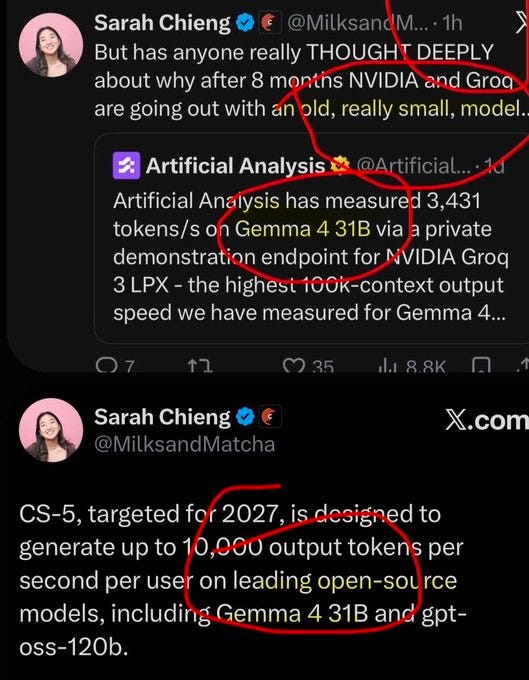
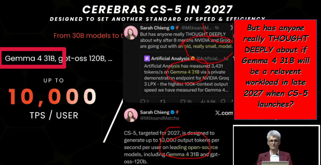

How do you think Feynman + future LPU is gona look like after Nvidia/Groq have time to make a real product from scratch instead of panic polishing an existing turd?
This leads to my core argument, multi-vendor disaggregated inference is a temporary anomaly. Everyone will try to go vertical.
Let’s go socket-by-socket.

Disagg inference requires a lot of co-design on software and networking. Even after all of that, deployment (is this even a good idea) is in question.
Recently visited one of my smartest and most trusted friends in SF. He is an expert accelerator programmer with direct experience at serving inference at massive scale. We spent a long time discussing these two OpenAI Jalapeño slides.
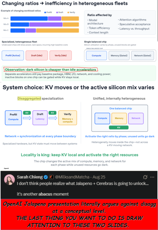

My genius-level friend agrees with OpenAI’s arguments whole-heartedly. In fact, he reminded me of a conversation we had a year ago on this topic that I did not understand at the time.
The problem with AI inference is the workload is quite dynamic. In the span of 1-3 months, you can see drastic swings in request patterns.
More/less reasoning tokens.
Wildly different input vs output token sequence lengths.
Shifts from models that are more compute of memory bound.
New attention strategies.
My friend and OpenAI make the exact same argument. The datacenter gets built for years of operation. He says 6-years, I still think useful life of accelerators is 3-years and people gona rip out and throw away Blackwells to replace with Feynman but that is a topic for a different day.
If your workload is drastically shifting every 1-3 months but the datacenter needs to be useful for 3-6 years, how the fuck do you plan the heterogeneous hardware deployment, topology, and load balancer?
Dark Silicon is cheaper than idle accelerators. — OpenAI
The conversation around disagg inference seems very distorted by delusional hope. There are many startups who WANT to believe they have an opening and thus MUST pursue multi-vendor disagg support. I believe everyone except Cerebras is wrong in pursuing this.
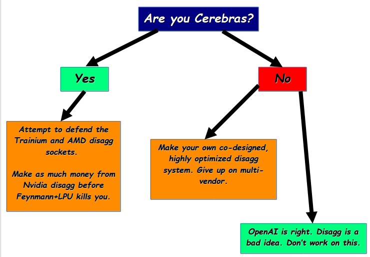
Throughout my career, I watched people far smarter than me make wrong decisions due to bias, even when massive red flags indicate that their thinking is fundamentally flawed.
I see a lot of cope and hope surrounding disagg. If this section is a little confusing sorry. Trying my best to distil the long technical discussion I had with my trusted friend last week. I am a hardware guy so don’t fully understand what he told me but understand enough to realize what OpenAI publicly declared in their Hot Chips 2026 presentation (with respect to disagg inference) is huge, comically under covered, and perhaps intentionally ignored because of what it means to your hopes and dreams.


🙈🙉🙊
[9.b] AI acceleration of chip design is real but not in the way the cultists want you to believe.
OpenAI Jalapeno has crated a mystical narrative that I hate. Funny how multiple people can see the same things but make wildly different conclusions depending on bias. In a way, people tend to see what they want to see, fill in the gaps, anthropomorphize.
AI as a technology is uniquely able to make people THINIK it is smart.

Remember that Google employee who got fired over going full AI-psycho over… LaMDA, a fucking braindead retarded LLM from mid-2022.
People keep forgetting that the ‘A’ in “AI” stands for “artificial”. It’s not real. Artificial means fake.
This section took the longest. Spent a lot of time thinking on how to structure. Mildly concerned this is still going to end up unintelligible even after all this effort and several re-writes but oh well an attempt was made.
Let’s start with a couple of history detours.
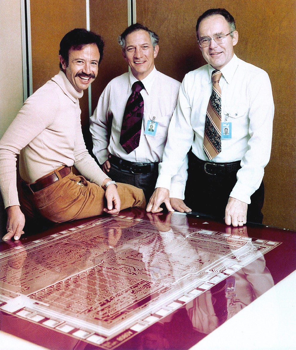
This is a famous picture of the Intel co-founders, Andy Grove, Robert Noyce, and Gordon Moore. Many have seen this picture but few of you probably know what the red-maskish thing is front of them.
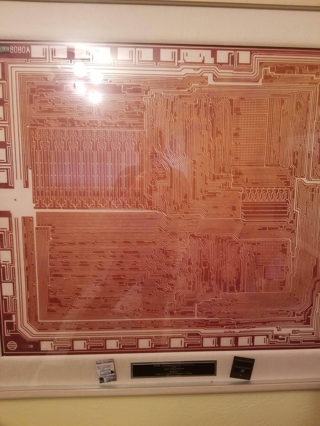

It’s a rubylith mask of ONE LAYER of the historic Intel 8080 CPU, originally launched in 1974. 50 years ago, EDA tools did not exist. All chip design was done by hand.
In the modern day, we have electronic design automation (EDA) tools that perform work billions and billions times faster than human engineers in the 1970’s. These EDA tools run mostly on CPUs, FPGAs, and ASICs (Cadence Palladium). These same tools are used to make new and better CPU+FPGA+ASIC.
Has the productivity enabled by EDA software tools grown exponentially in the last 50 years? Yes.
Have we entered a recursive singularity where EDA tools have made the god-CPU that ends all CPUs? No, what the fuck are you smoking, cultists?
AI has transformed chip design. The last 2-3 years of AI progress have led to 5-10 years of effective/traditional EDA progress. Will give some heavily-obfuscated real-world examples shortly.
In my first year of grad school one of my professors gave a 10-minute speech on extrapolation. He was a very old man, spoke slowly. Had to re-watch his lecture at 1.5x speed so this speech was really 6.7 minutes long on an adjusted basis.
This speech can be distilled down to “extrapolation is bad, if you have a lot of data maybe you can extrapolate one order of magnitude, maybe two, but not 5.”
At the time, I was confused as to why this professor was wasting so much time on something this obvious. Everyone knows this… right?
Apparently not. 9 years later I live in a world surrounded by people who enthusiastically extrapolate exponential curves and derive their entire world-view, identity, and psyche around such extrapolations of exponential curves.
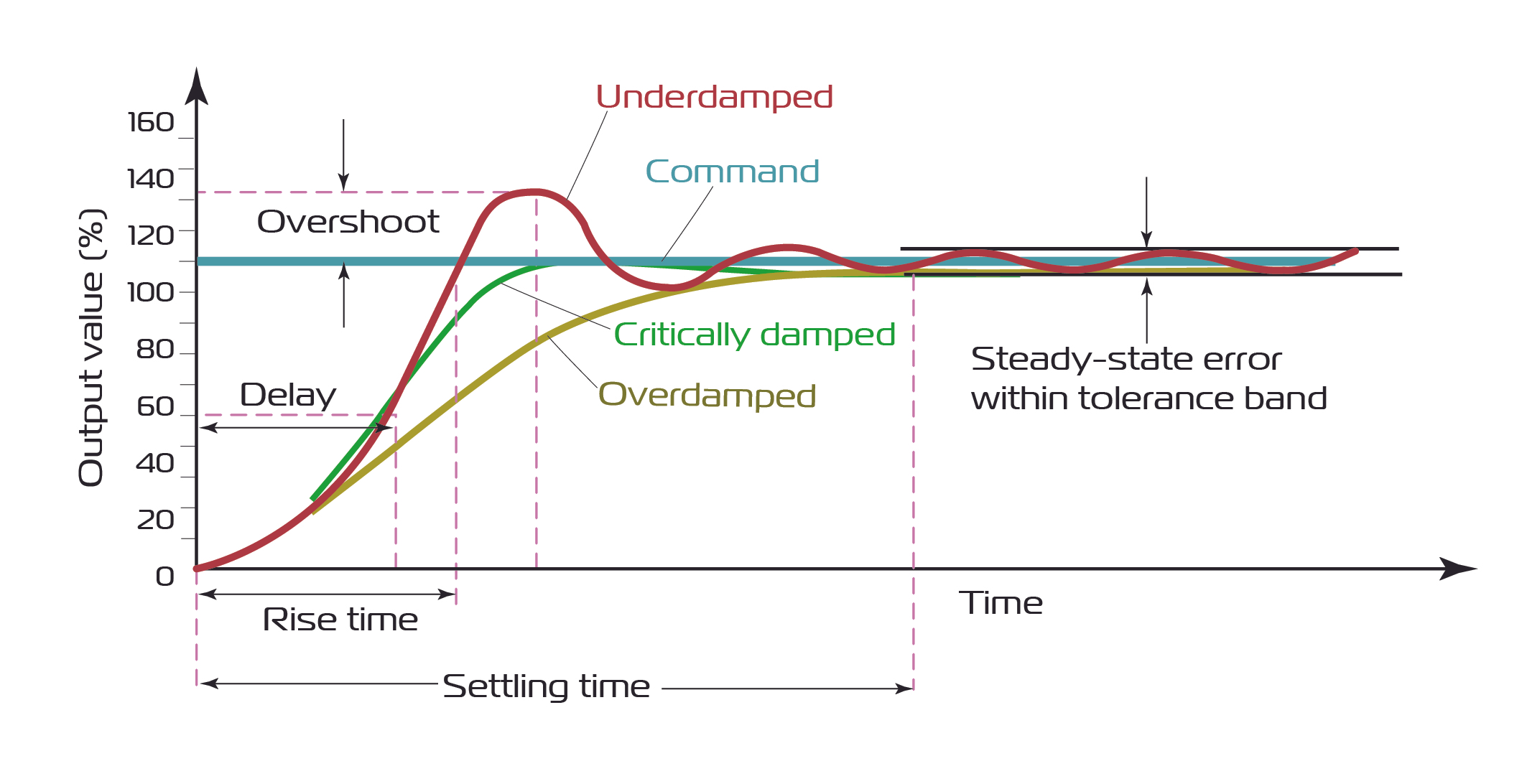
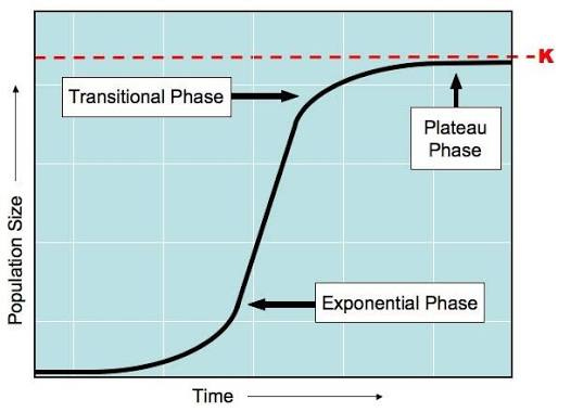
Real systems don’t stay exponential forever. Something always stops it. Could be an engineering force, or maybe a societal force.





I find it amusing (in a detached and somewhat psychotic way) that the AGI cultists spend so much time fearing AI when they should be very afraid their fellow human.

But enough of this. We are drifting off-topic. There is a half-finished draft post that has been languishing for over a year. Maybe someday it will be published.
A long time ago, differential equations were calculated with analog computers.
https://en.wikipedia.org/wiki/Differential_analyser
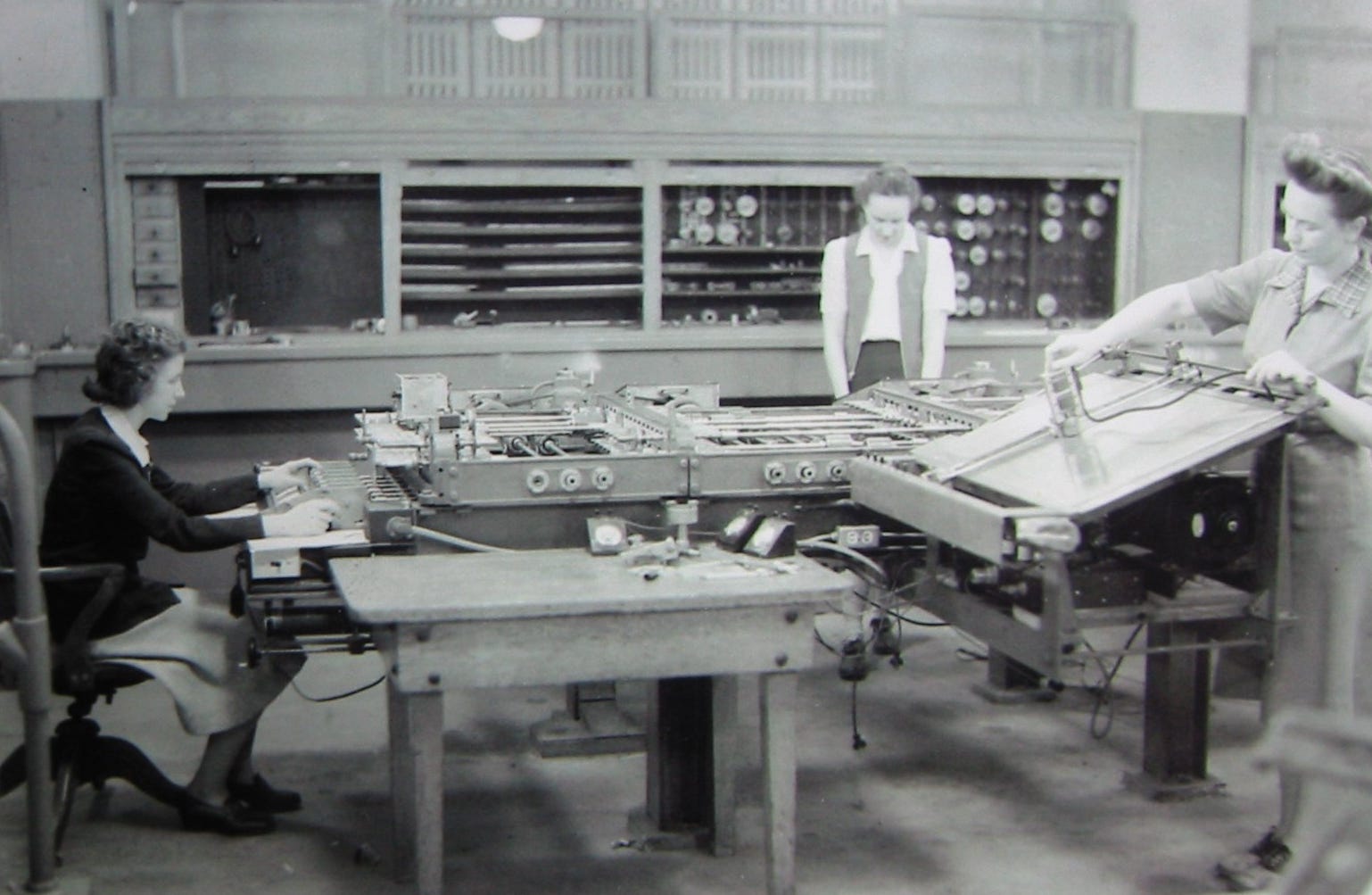
Humans operated these machines to calculate trajectories. Useful in war and space exploration scenarios.
Nobody calculates differential equations by hand or with mechanical tools anymore. We have digital computers that are unfathomably faster.
Tools are great. Why has most of the San Fransico Bay Area lost its mind and started projecting their entire psychology and identity into obsessing over and worshiping a set of new tools?

There is something deeply wrong with society at this place. There is truly no good way to describe it. You have to live here continuously for at least 6 months to understand how broken the people are here. (I am one of them to be clear, just broken in a very different way.)

There is one detail in the Semianalysis coverage of OpenAI Jalapeno that stands out as a massive red flag. Amusingly, this detail is portrayed in a positive light which is completely wrong and makes me question if anything in that note can be trusted.
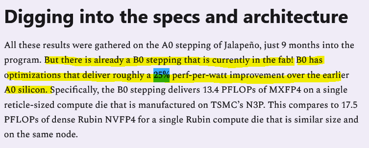
If your B0 stepping is 25% faster than A0 at ISO power, it means there was a catastrophic problem that got fixed.
A 5-10% improvement means designers got in a few last-minute features and fixes in.
A 15% improvement means a serious problem was fixed.
A 25% improved is frankly just as bad as a 50% improvement in terms of what it means for your initial silicon (A0) design. It means either you fucked up badly or the Foundry fucked up badly. Those of us who have interacted with Samsung Foundry back in the 5LPP/4LPE/4LPP days know what it’s like to get a PDK that is completely wrong.
In this case the process node is TSMC N3P, the worlds best leading-edge process node in terms of PDK quality. So it seems that OpenAI vibe-coded their chip and botched it.
There are many ways of cheating at a silicon level.
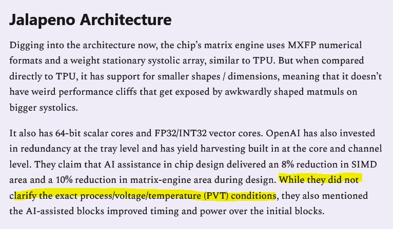
Do I sound like somehow who knows how to fake demos?
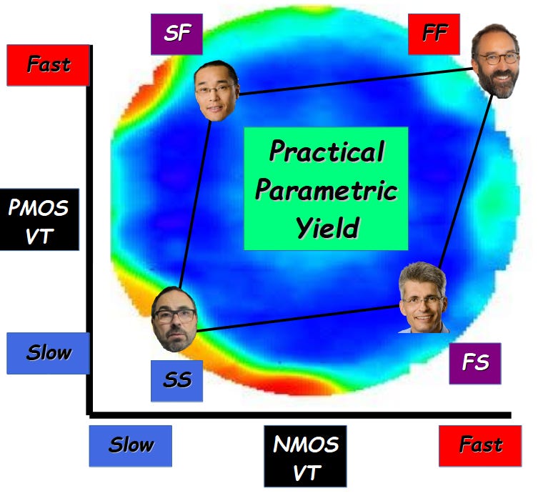
It takes someone who knows how to cheese to spot cheese. More on this in the practical parametric yield deep-dive.
For now, I would like to raise a rather obvious non-technical question.
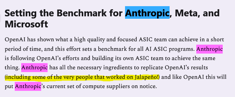
Clive Chan, the most important person from the Jalapeno team, left. He is a genius-level guy for hardware-software co-design.
At least 10 other engineers who were on Jalapeno also left.
Tell me, what is the typical conclusion to seeing massive attrition from a project? Obviously the project went well, there was no catastrophic fuck-up, and that 25% perf/watt boost from a full re-spin is because AI is so good, not because the original design had a disaster-level problem.
I want to end this section with some heavily obfuscated real-world examples.
[1]
Digital logic (RTL) designers use tools to view waveforms. Looks something like this.
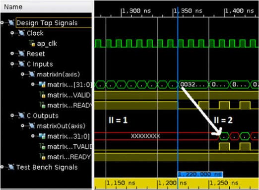
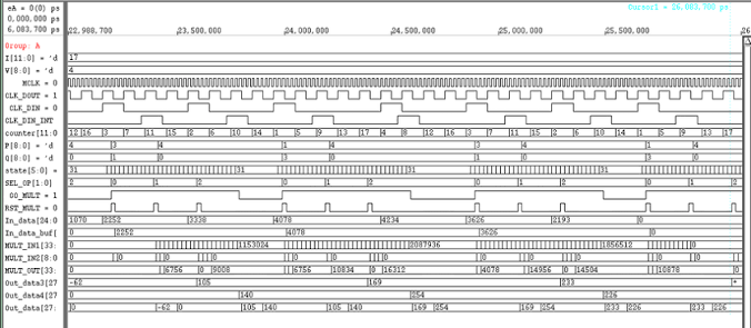
Pulling up waveform files to debug is a tedious thing. These days, a small percentage of RTL engineers don’t pull up the waveforms at all. They have an AI agent read the waveform (dumped into text), do the boring and tedious initial investigation. Then the human designer reviews the “points in the right direction” from the AI agent and figures out what the problem was and fixes it.
For relivable tasks (coding) AI is massively accelerative. Applies to regular software (C++) and RTL (System Verilog).
Teams of 3-7 good/competent engineers are accomplishing work that would normally take 20-30 engineers in half the time.
But it’s not all sunshine and roses. AI often makes incredibly stupid decisions that no human would ever make, cheats, or simply refuses to obey direct instructions.
AI can also have very negative consequences. There was this time where a co-worker who is much smarter than me came asking for help. He showed me this very long AI chat where he fed a small chunk of the chip design and was trying to get help on how to design the algorithm to control that chunk.
The AI output was quite long. He probably spent at least an hour talking to it. There were the beautiful diagrams and equations. So many fancy words I did not understand.
But it only took my dumbass 90 seconds to realize he fed the wrong part of the chip into the AI. All of that beautiful output was confided slop. Completely wrong. AI just kept going, vomiting bullshit and wasting the engineers time.
Within another 90 seconds I opened up the chip in KLayout, found the right sub-circuit, and told this guy everything the AI told him was bullshit and he should start from scratch.
A family member of mine is a very experienced petroleum engineer. He complains about how the “young people” are obsessed with simulation software and have zero critical thinking skills.
Idiot, if the pipe pressure is negative maybe something is wrong. Is the oil going to flow backwards?
A base-level of understanding of a subject is necessary. Give powerful tools top a tourist and they will have no idea of the tool just outputted garbage.
Earlier this year, I was discussing a technical matter with a friend. He started to copy/paste AI generated text that was completely wrong. I would correct one round of outputs and he would quickly prompt again and send me more dogshit slop.
Eventually I got frustrated and just ended the conversation with my human friend because he was being completely useless. Even after several detailed explanations on why the AI output was wrong, he still kept prompting more crap. Maybe recognize the AI is outputting garbage and start thinking for yourself or admit you have zero understanding of the conversation topic?
[9.c] DRAM vendors have overplayed their hand.
Gross margins are a funny thing. Too high and everyone knows they are getting screwed. Too low and everyone attacks the suppliers out of opportunity.
DRAM vendors hiked to well above 80% gross margins, so everyone is pissed. And there is not nearly enough supply, which makes everyone extra pissed and forces evaluation of ANY AND ALL alternatives.
My sense is the DRAM vendors (correctly) saw HBM as an opportunity. A special opportunity to let the customers kill each other.
HBM demand destroys more bits/supply.
Higher-end HBM (more layers) destroy even more bits/supply.
HBM customers keep demanding more capacity…. until they don’t.
One of the major conversation topics of Hot Chips 2026 were all the HBM de-spec rumors. It seems everyone wants LESS HBM. Well, fewer layers per stack but still buy as many stacks as possible.
It’s never a good sign when customers ask for lower-end versions of your product. It means they found a way around you and your roadmap has less value-add than you think.
Which is not to say memory stocks are bad. I own a rather large long position in Samsung in the long only accounts.
Just want to point out that the situation was perhaps not optimally played.

[10]Full Portfolio Update: 9/5/2026
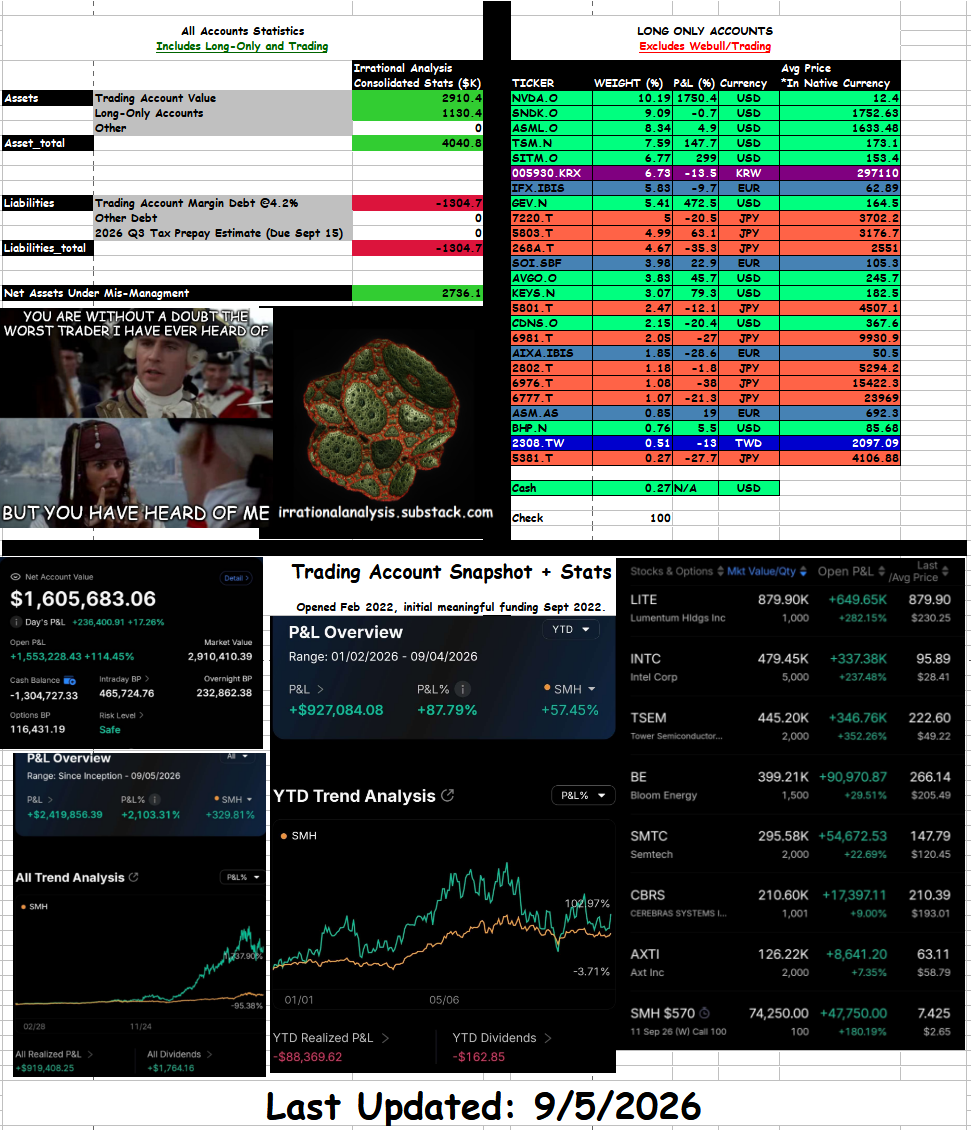
My goal is to outperform my benchmark (market-cap weighted semis index) SMH 0.00%↑ by at least 30%. Presently exceeding this bare-minimum goal by only 0.34% which is frankly embarrassing but hey there are three weeks left in this quarter. I have time to make some of the lost gains back.
This one took forever and I am very busy with dayjob. Will take a break then start working on practical parametric yield deep-dive. Have not been this excited to write a technical deep-drive in a long time. But also exhausted.
Great write up as usual. Very interesting even for us that only understand some of it.
The GOAT has spoken