
High Voltage, Low Competence
SiC vs GaN , HVDC, and the future of datacenter power.

Irrational Analysis is heavily invested in the semiconductor industry.
Positions will change over time and are regularly updated.
Opinions are authors own and do not represent past, present, and/or future employers.
All content published on this newsletter is based on public information and independent research conducted since 2011.
This newsletter is not financial advice and readers should always do their own research before investing in any security.
Feel free to contact me via email at: irrational_analysis@proton.me
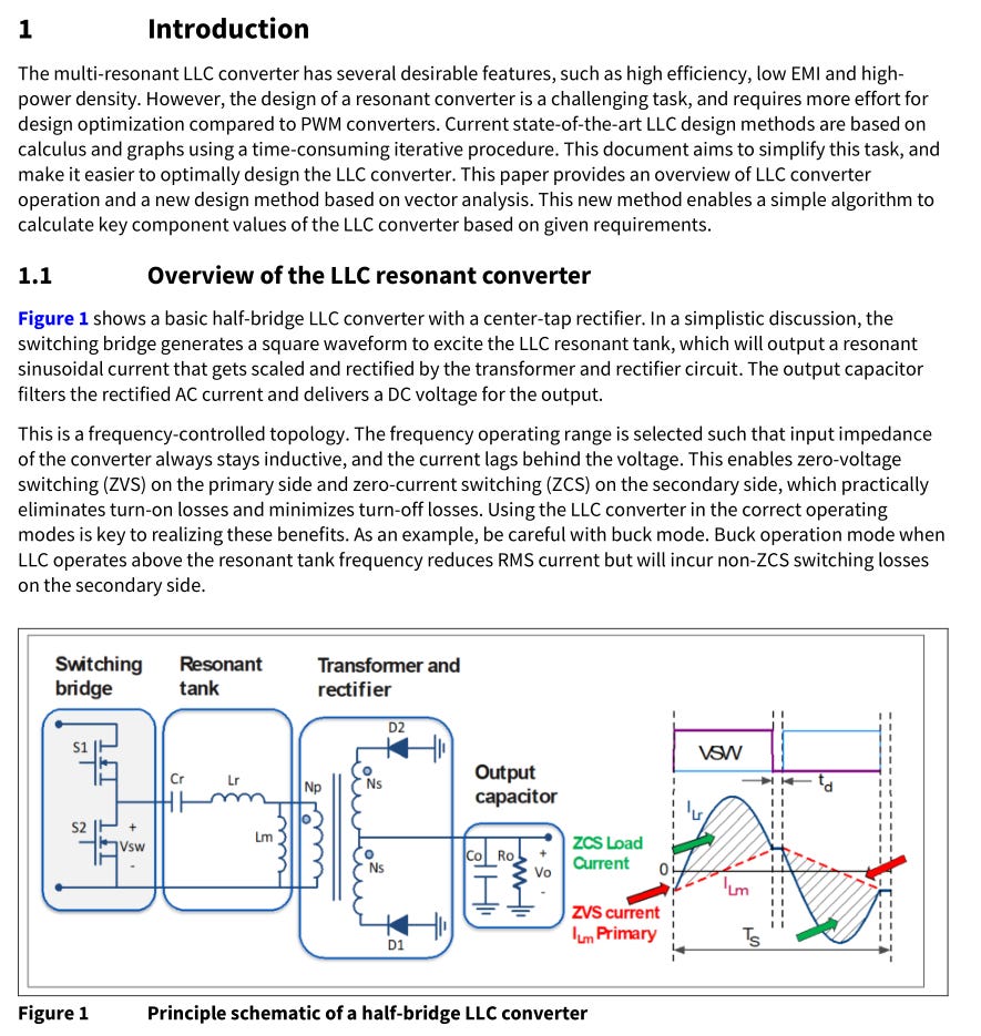
Welcome to a very exciting project on high-voltage power semis (SiC + GaN). This entire industry has been eating shit from EV/automotive downcycle and Chinese competition.
Whats super awesome about this space is the above two major negative factors are irrelevant to the sector going forward in my opinion.
Broadly speaking, power semis are all about tradeoffs between the following factors:
Footprint (how big circuit is)
Conversion Efficiency
Control complexity.
Switching Frequency vs Voltage (effects above three)
In EV/automotive, you can compensate for lower efficiency with a larger battery. There is enough space/footprint to make cheaper SiC parts work economically. Thus, you get a race to the bottom which we have seen.
Datacenter and power grid markets are the opposite. Every last shred of efficiency matters. Footprint is critical. You either fit in the power sidecar rack or you don’t. And due to national security and supply chain risks, Chinese parts on the USA power grid is not gona fly with Trump. You can bet the Hyperscalers who are desperately trying to prop up domestic transceiver manufactures ([LITE, AAOI, COHR] over the Chinese [Innolight/Terrahop, Eopto, Accelink]) are putting the same pressure on the power module supply-chain.
This entire market is moving from a knife fight between retards who over-built (looking at you Wolfspeed) and Chinese players with 30-40% lower cost to a quality-based pricing regime where demand is going to vastly out-strip supply by H2 2027, if not earlier.
The best part is, all the datasheets are public! Was pleasantly surprised by this as the low-voltage switching regulators tend to have private datasheets to prevent easy analysis of “who has better part”. A friend told me these high-voltage parts have public datasheets due to regulatory/safety reasons so horary for red tape for once that shit is useful.
Over 10 years ago, I got destroyed in my first upper-division undergraduate analog design class. Spent 50+ hours per week on JUST THAT ONE CLASS, practically lived in the shitty lab where we built test circuits on breadboards and simulated on PSpice. Failed the final exam because my dumbass forgot a resistor and ended up designing an amplifier that tied output to ground. TA gave me 10% on that design problem because my frequency domain analysis of transistor parasitic capacitance was correct. Got a B- (others failed harder than me) and pivoted entire life/career. That one class killed my dream of becoming a chip designer. Realized no matter how hard I tried, I could never be good at chip design. Pivoted to digital signal processing, the opposite sub-field in electrical engineering.
So… I am completely un-qualified to write about this but gona try my best anyway. It’s funny how life turns out. Can’t design circuits but I can read datasheets, play with existing simulation files, and make money trading/investing in analog semis.

Contents:
SiC vs GaN: The Pointless Argument
Tour of Sample Circuits
500V DC to 200V AC (1-phase)
200V + 200V DC to 115V AC (3-phase)
800V DC to 12V DC
800V DC to 50V DC
Key Points
Transistor Attribute Crash Course
Datasheet Comparisons
GaN+SiC 650V-class
SiC 1200V-class
SiC 1700-2000V class
Wolfspeed 10KV Madness
Driver Integration, Protection Circuits, Buffers == VALUE
Multi-Sourcing, A Practical Perspective
EPIC OPPERTUNITY: Solid-State Transformers
Public Market Investment Corner
[1] SiC vs GaN: The Pointless Argument
Many companies in this world are biased and spout bullshit claims that have no technical merit.
Let’s start with this excellent slide from WOLF 0.00%↑.
The chart itself shows the key design tradeoff between SiC and GaN.
GaN enables higher switching frequencies.
SiC enables higher voltage and power density.
Wolfspeed has no GaN exposure so they try their best to shill SiC as a better market. This is bullshit.
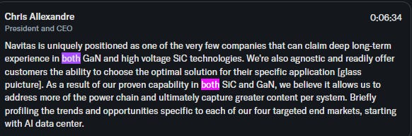
Conversely, Navitas is far more levered towards GaN and tries to shill that as much as possible. Also bullshit.
Finally, Navitas CEO likes to claim that it matters that they have both SiC and GaN and this is somehow an advantage. Complete bullshit.
Nobody gives a damn if one company can offer both. Designers will chose the best SiC and best GaN parts for the situation. Literally nobody cares if both parts come from the same company.

By the end of this post, you will understand:
The tradeoffs between SiC and GaN.
Why both have significant value.
Who has the best SiC.
Who has the best GaN.
How circuit designs enable multi-sourcing and the limits around these strategies.
You gona want exposure to both SiC and GaN.
Let’s get started!
[2] Tour of Sample Circuits
My original goal was to build some sample circuits and simulate multiple parts against each other. Very quickly realized this is not going to happen.
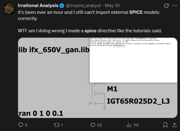
Simulation software for this kind of thing is called SPICE. PSpice (Cadence) is the industry standard. LTSpice (Analog Devices) is free so I am using that.
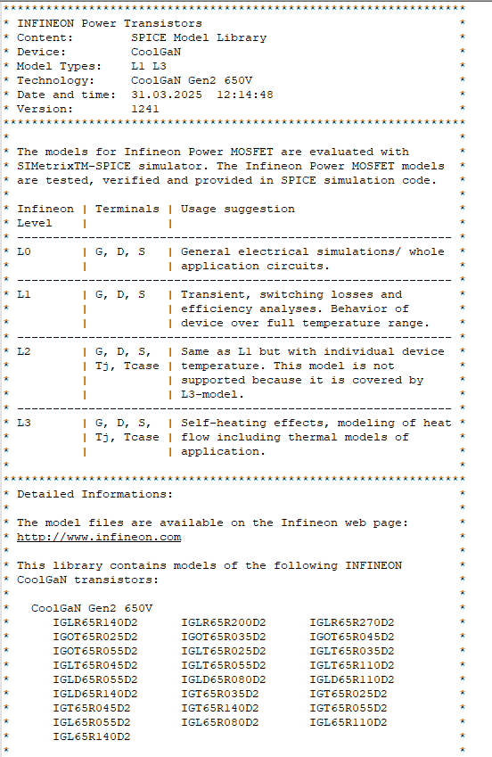
Vendors provide models for their devices. For example, here is the SPICE model for Infineon 650V-class GaN discrete MOSFETs.
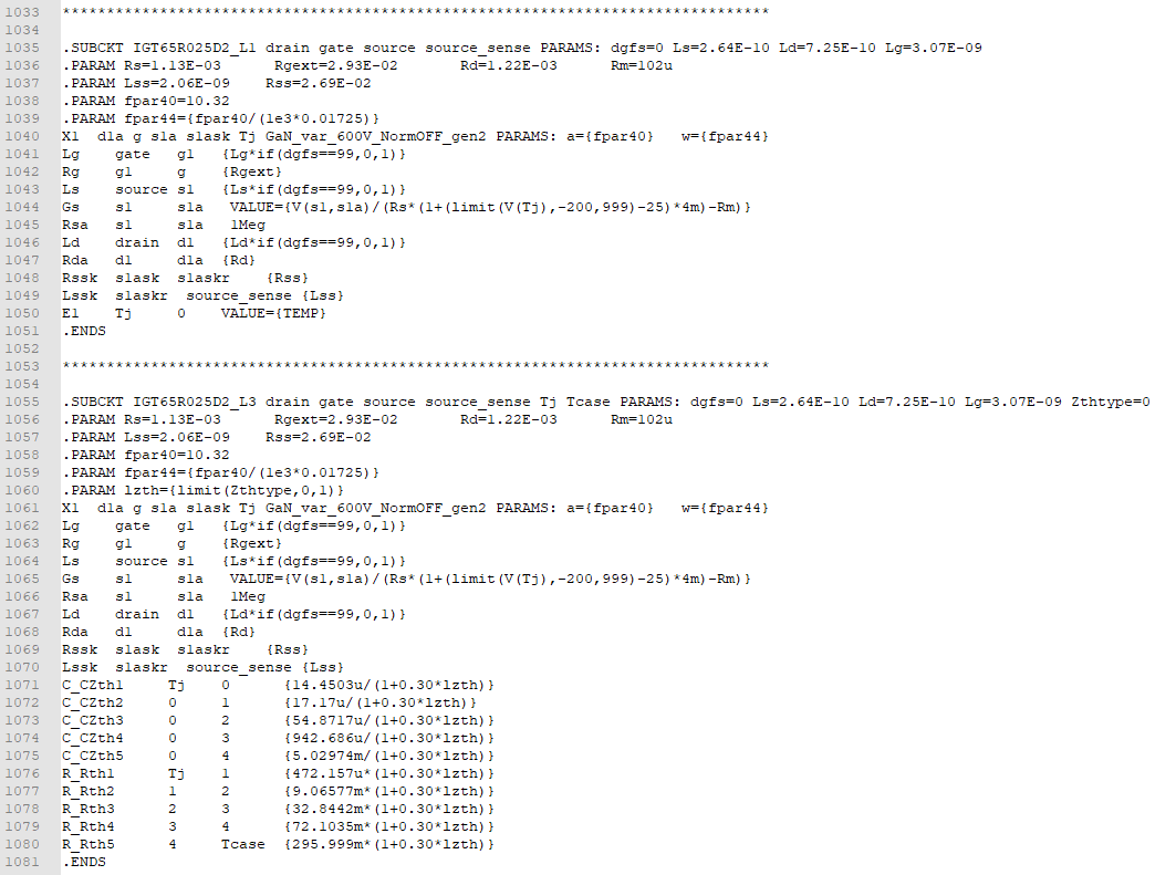
The part I was trying to import has this model.
If I am too dumb to import a model, I absolutely can’t design a circuit based on YouTube tutorials.
And so, the search began for some pre-made LTSpice schematics. Found a glorious resource from ROHM semiconductor.
https://www.rohm.com/support/ltspice-circuit
Full, ready to run schematics with detailed PDF guide on how to edit the parameters. Exactly what I needed.
The rest of this section is a walkthrough of some of the ROHM sample circuits. My goal is to build your intuition before going into more technical details.
I highly encourage all of you to download LTSpice (free!) and these ROHM files and play with them yourself. It’s easy! Even a midwit boomer PM like Brad Gerstner could set this up.
https://www.analog.com/en/resources/design-tools-and-calculators/ltspice-simulator.html
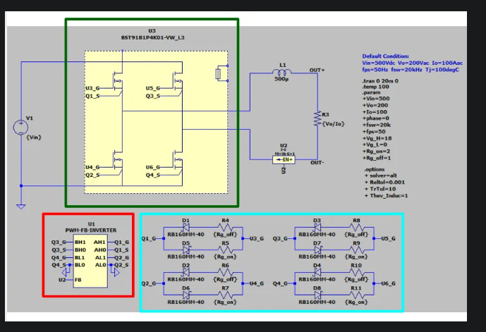
[2.a] 500V DC to 200V AC (1-phase)
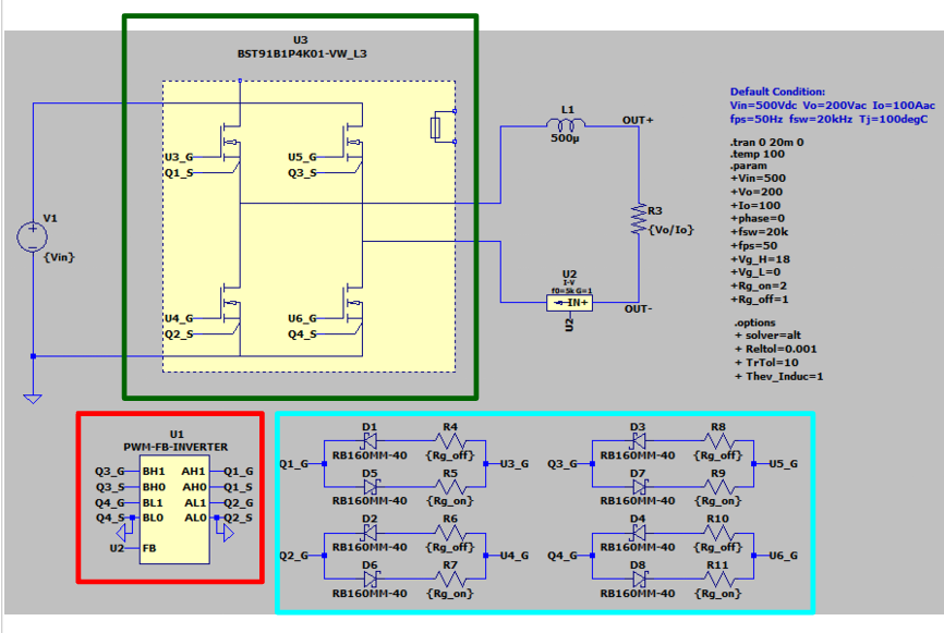
Let’s start with the red box. This is the PWM controller. Thing that sends the signals to control when the SiC transistors (green box) turn on/off.
Opening up the SPICE model shows this…
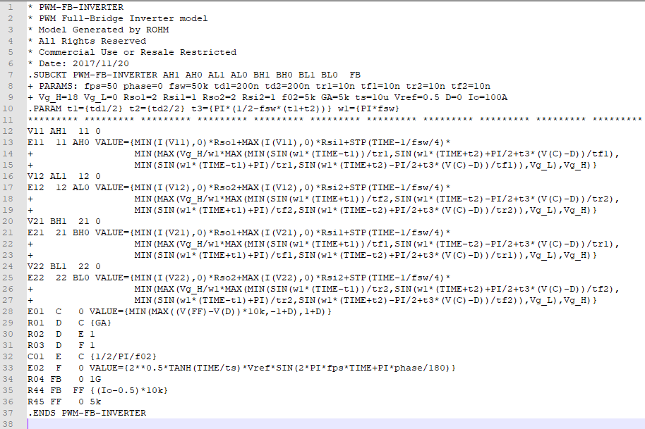
It’s just a bunch of hardcoded math. In the real world, more sophisticated control algorithms are sometimes needed. Depends on the ripple/stability/temperature requirements.
Blue box is just basic protection circuitry using some Schottky diodes. Prevents the transistors from frying the controller and vice-versa.

Let’s run the simulation and probe different parts of this circuit.
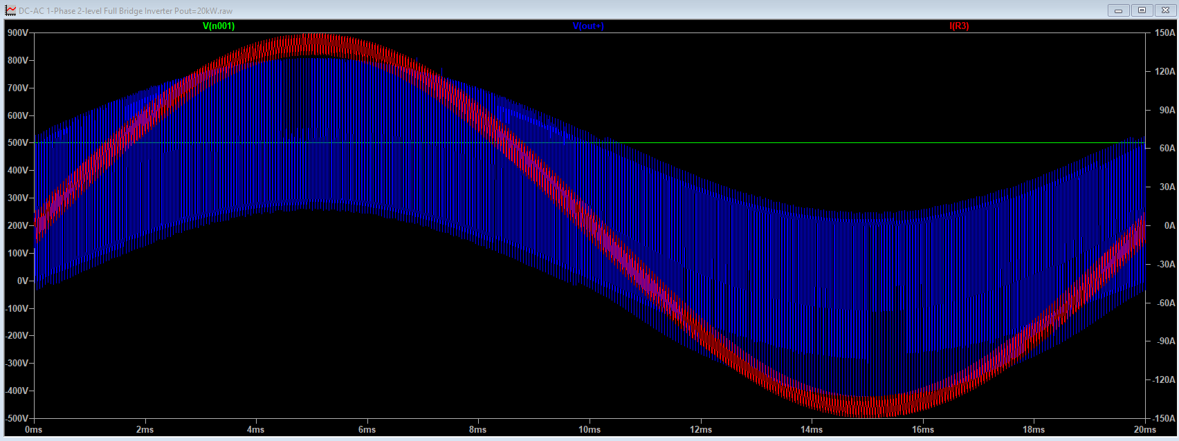
As you can see, voltage input (green) is perfect/flat/ideal 500V DC.
The output is 200V AC. Notice how there is ripple. This is undesirable and must be controlled within a certain tolerance depending on the application.
If the DC source was not a perfectly flat 500V, this ripple would be even worse.
Hint: the real world does not have ideal voltage sources.
[2.b] 200V + 200V DC to 115V AC (3-phase)
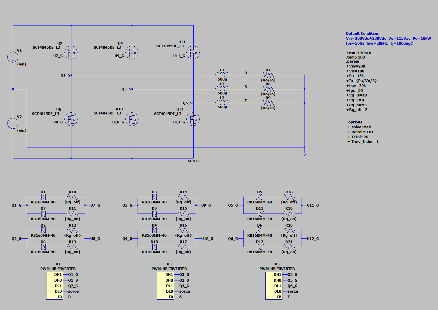
Here is a 3-phase DC to AC converter. You will understand what this means shortly.
Notice there are three controllers. You can build a single larger controller chip but for the purposes of managing the simulation, it’s easier to just make three small controllers.
Let’s probe the output current across the three load resistors.
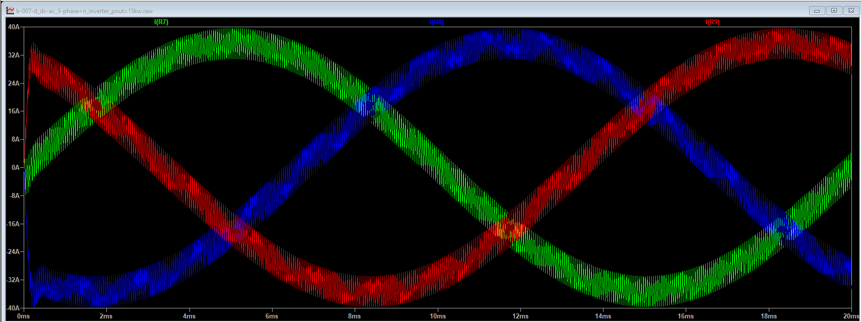
Three AC signals at a 120-degree offset (slight time delay) are generated.
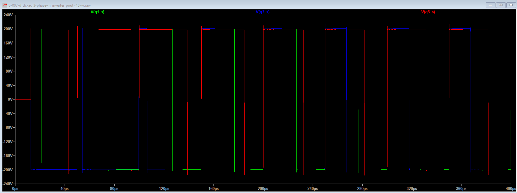
Probing the nodes between each pair of transistors, you can see the switching action. How the transistors turn on and off to generate a square wave.
[2.c] 800V DC to 12V DC
Now to a more interesting circuit. 800V DC direct to 12V.
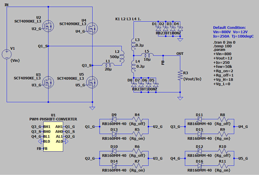
See how there are two halves to this circuit, separated by inductors? This is called isolation. It’s a safety strategy.
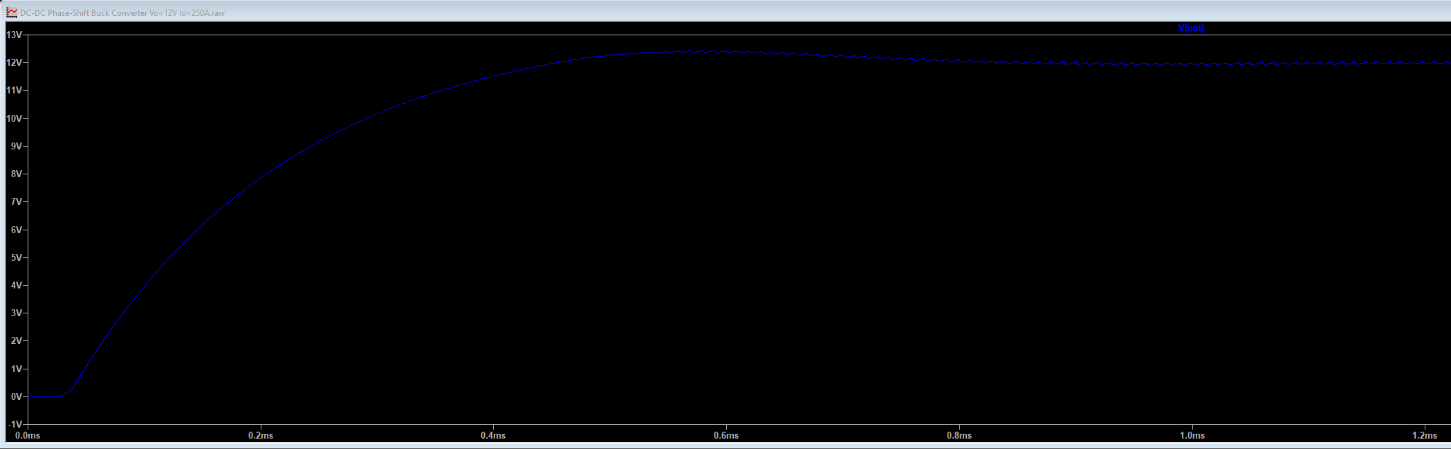
It takes time for the output voltage to ramp to 12V target.
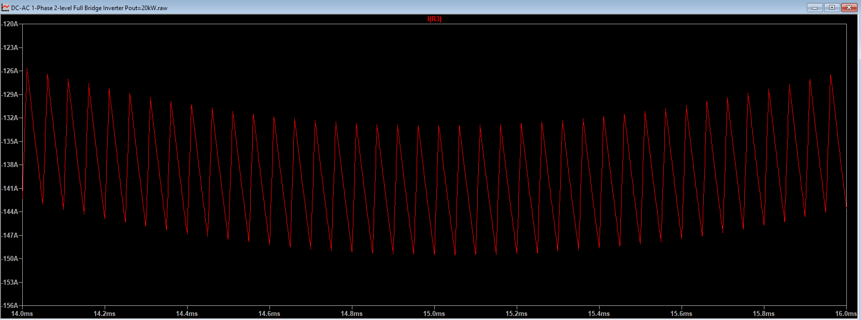
Zooming-in, you can see the ripple.
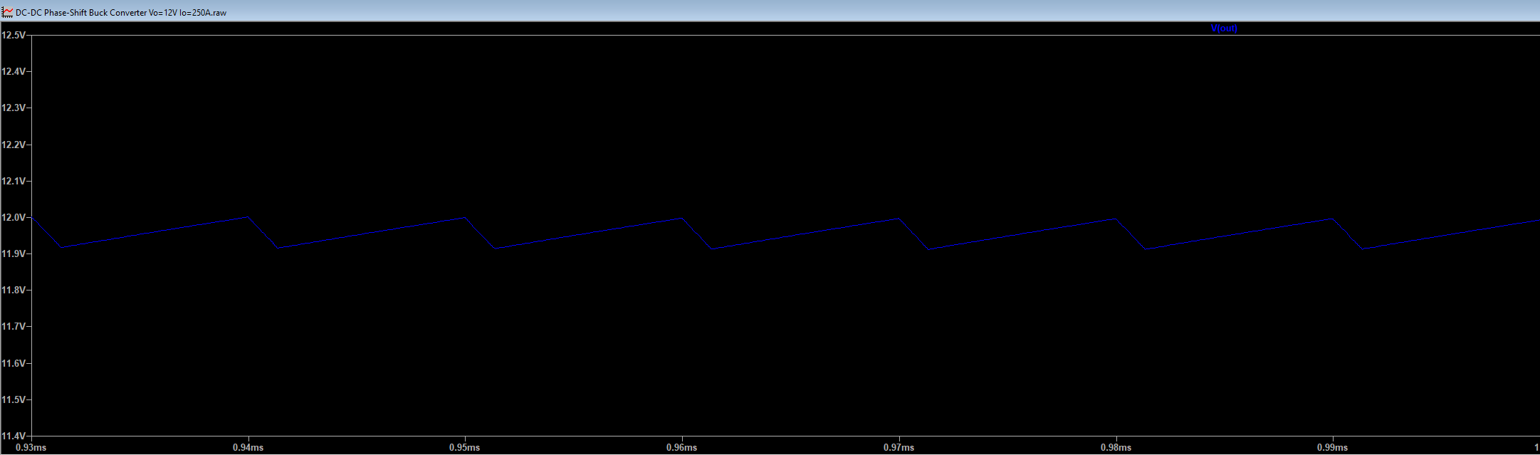
In this case, the ripple is only +/- 50 mV which is pretty good given the power conversion ratio. But remember… the 800V voltage source is ideal. In the real world, input ripple/noise is amplified. Output filer design is critical.
The output filtering of this schematic is quite basic. Handful of inductors and diodes.
Output filtering can become much more complex with higher-order LC filters and de-coupling capacitors.
[2.d] 800V DC to 50V DC
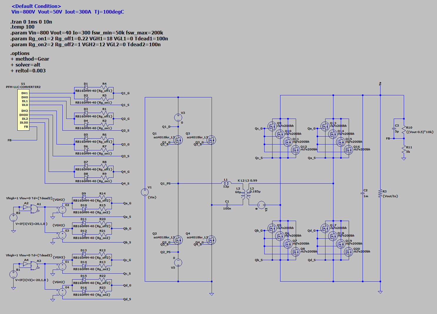
This one has two important concepts. Notice how the transistors on the left half are labeled “sct”, aka subcircuit. They are in fact, TWO transistors stacked on top of one another.
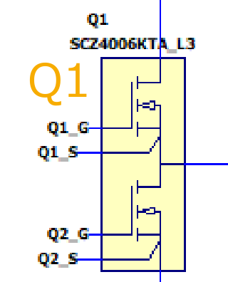
This is because there is too much voltage across this node for one SiC transistor to handle.
Looking at the ROHM datasheet…
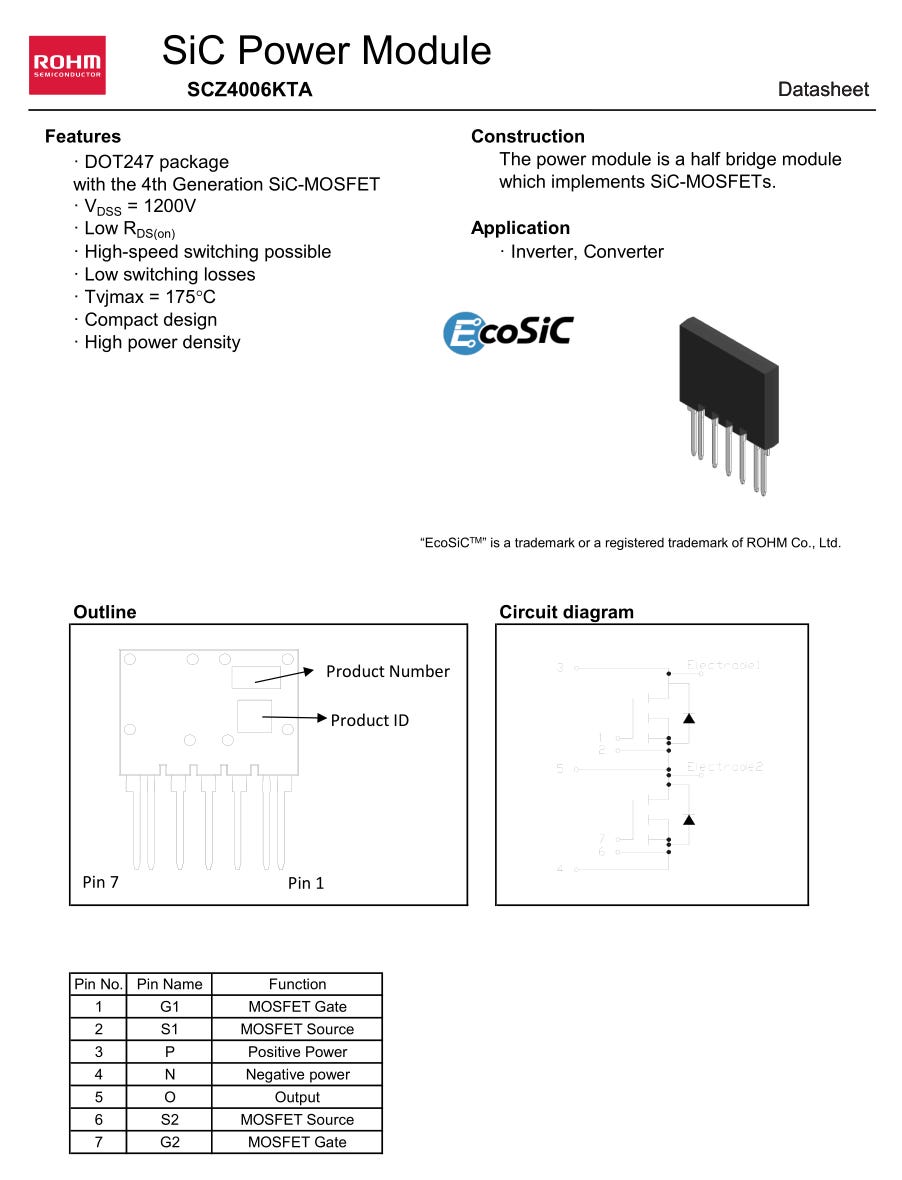
It’s two 600V-class transistors shoved into one (fat) package to give a device that has 1200V rated max Vdss. Obviously there will be more parasitic resistance and you have to control two gates but hey it works. The alternative is 600V rated transistor go kaboom.
Similarly notice on the right side there are clusters of four transistors.
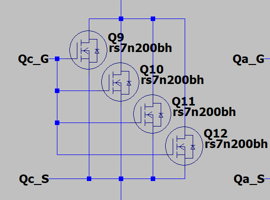
This setup is to get around the current limitations of the individual devices.
The design has quite a bit of overshoot at startup. 20%
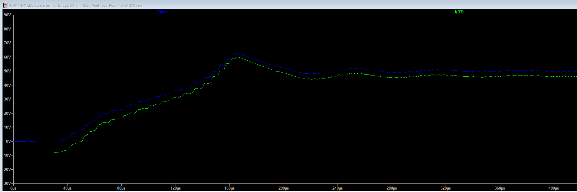
Overshoot can fry your load if you don’t plan things right.
[2.e] Key Points
Remember, the point of this section was to build intuition. Here are the key takeaways you need to remember going forward.
#1 Signal quality matters.
Overshoot can fry your load device.
Ripple can de-stabilize the system, making load devices unusable.
Input noise/ripple can be amplified by the power conversion circuit.
#2 Transistors can be chained to increase rated power/current/voltage.
Voltage too high? Just stack transistors in series.
Current (or power density) too high? Just stack transistors in parallel.
THERE IS A DOWNSIDE TO THIS. CONTROL COMPLEXITY AND EFFECIENCY SUFFER FROM THESE STRATEGIES.
#3 SAFETY IS CRITICAL. THIS SHIT IS DANGEROUS.
All of these demo circuits have only the most basic protection measures. Real products need MUCH MORE protection. The consequences of failure include but are not limited to…
Fire
Death of technician
Frying $10M+ of downstream or upstream equipment.

[3] Transistor Attribute Crash Course
Each of the upcoming datasheets is for a discrete MOSFET. One single transistor.
Turns out, it takes at least 5 pages of charts and 2 pages worth of tables to describe one transistor.
Only some of the datasheet is useful for our purposes. (PICKING STONKS)
For this exercise, I will use an Infineon datasheet because I like their formatting the best.
At the top, they have a table with key specs. They are all at 25C die temp which is useless but that’s why we have to go deeper with the charts later. One step at a time…
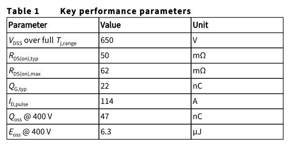
Vdss is the maximum voltage across the transistor/switch. You never want to be in a situation that is close to this number so it’s more marketing. In practice, a design will ensure less than say 500V for margin of safety.
Rds_on is the parasitic resistance and the MOST IMPORATANT SPEC. When the transistor is on, it ideally should be a perfect short circuit. In reality, there is some parasitic (unwanted) resistance that directly leads to power efficiency loss and heat generation.
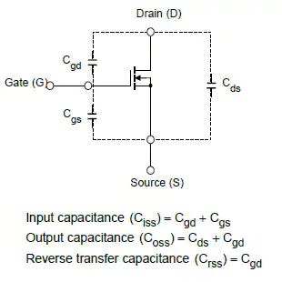
Qg is gate charge. This is another parasitic effect. Gate is the control pin. Unwanted capacitance at that pin means it takes longer for the transistor to switch between on/off.
Id_pulse is the maximum instantaneous current that can pass through the transistor. Like Vdss, you don’t want to be anywhere near the max for safety reasons.
Qoss and Eoss is capacitance/energy stored/dissipated by the transistor. This is bad because that energy is wasted every time you switch from on/off or vice versa. Notice how these two specs are quoted at 400V even though the transistor is rated for 650V. YOU NEVER WANT TO BE ANYWHERE NEAR MAX RATING. SAFETY SAFETY SAFETY.
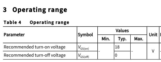
All transistors have a threshold voltage (minimum voltage needed to make it start turning on) and a recommended voltage for operation.
In general, lower gate voltage requirement is better. Simplifies control circuitry design and efficiency.
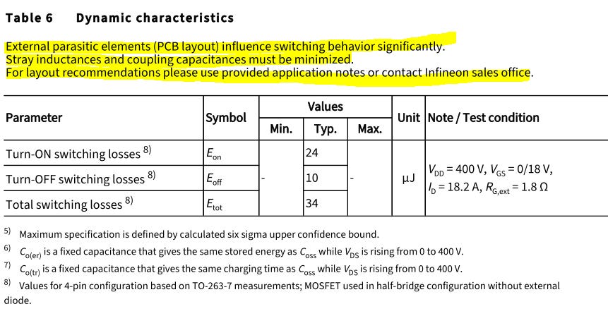
Switching losses == wasted energy
As you can see from the warnings and many asterisks, a lot of factors can mess with performance. Designing quality PCB and supporting circuitry is difficult. Easy to fuck this up.
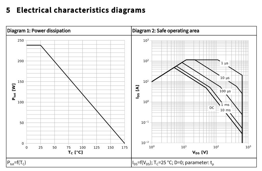
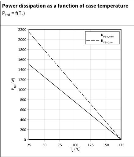
Maximum power dissipation is directly linked to temperature. This is why the numbers are 25C are useless and you have to read the charts. There is no reality in which these parts will run at 25C at nominal conditions.
Safe operating area is determined by three factors:
Switching speed (faster means transistor is stressed for shorter bursts so you can push it harder)
Voltage
Current
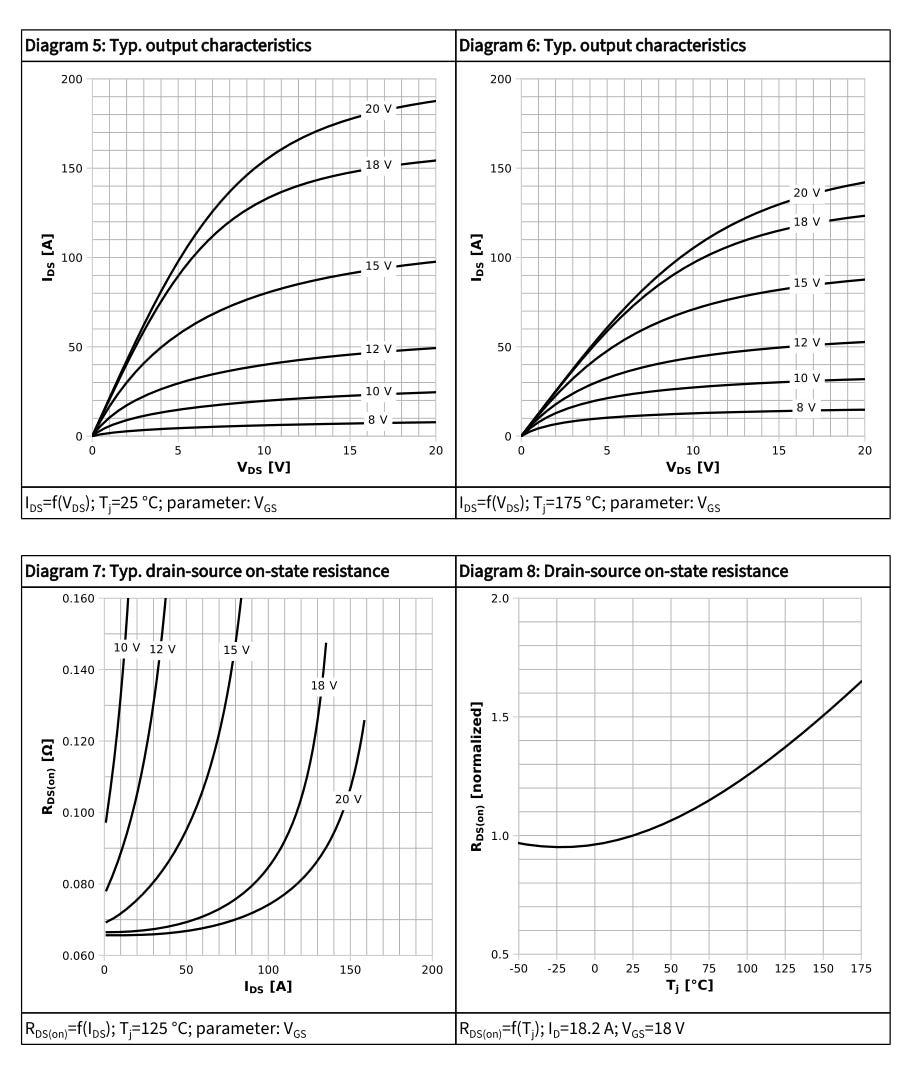
Each curve corresponds to a gate drive voltage. Remember that Infineon recommends a drive voltage of 18V for this part.
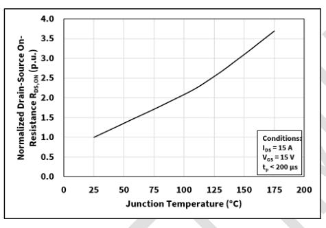
Parasitic resistance varies due to many factors, but the one we care about the most is temperature.
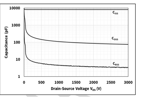
Also handy reference for parasitic capacitance.
[4] Datasheet Comparisons

For the purposes of this set of comparisons, I will attempt to make the playing field fair.
General Rules:
Only compare discrete MOSFETs. (no compound devices such as half bridge)
Chose the lowest Rds_on part from each vendor.
Group by voltage class.
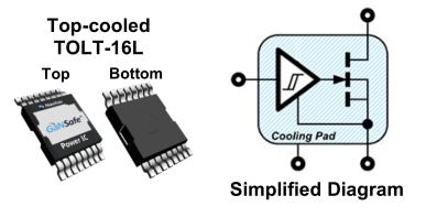
Must be in appropriate package for the target market. (TOLT preferred)
Each section will also have a target die temperature picked somewhat arbitrarily by me. Comparisons at 25C are retarded so me picking some higher temp at random is still better.
[4.a] GaN+SiC 650V-class
GaN is currently limited to only this voltage class but ON 0.00%↑ vertical GaN might be real and enable GaN penetration into higher voltage classes. But for now, GaN stops here.
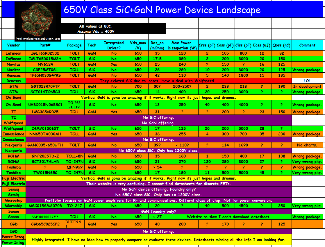
It took over 6 hours to make this table.

Many of the numbers are judgement calls from me staring at charts. Actual numbers in the datasheet are typically disclosed in inconstant ways or at useless conditions (25C case temp).
Quick comment on packages. TOLT is a style of package that allows for top-side cooling. Think liquid cooling of very dense power modules. TOLL (not TOLT!) is bottom side cooling where the PCB acts as a heat spreader. This is bad. Any package that does not allow for dense construction with topside cooling is categorized as “wrong”.
Let’s start with comparing GaN and SiC as a whole.
Broadly speaking, SiC can handle more power. This is expected. However, this comes at the cost of much higher parasitic and intrinsic capacitance. This means slower switching speeds, higher switching losses, and much larger inductors/capacitors/magnetics in full designs.
For 650V GaN, TI and Navitas are clearly in first place. Infineon is second place while STM has a competitive part in development but it is not ready. Once the new STM GaN part is ready, it will probably be tied with Infineon in second-place. Everyone else is far behind.
For 650V SiC, Infineon is in first place with STM is a close second place. Wolfspeed an On Semi are in a close third place. SiC world is more competitive.
I want to re-emphases a few points.
Both GaN and SiC can work well in the 650V class market.
Engineering is about tradeoffs. If anyone tells you only SiC or only GaN works in this market they are full of shit and biased.
It is irrelevant if one company offers both SiC and GaN. People will buy parts from multiple vendors based on quality and availability.
This brings me back to the mini-roast of Navitas CEO. Congratulations on having the worlds best GaN. Your SiC is shit. Why would anyone buy your SiC when Infineon, STM, Wolfspeed, and On Semi all have better parts?


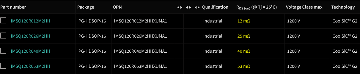
[4.b] SiC 1200V-class
Thankfully the higher voltage we go, the fewer players there are so these tables are less painful to make.
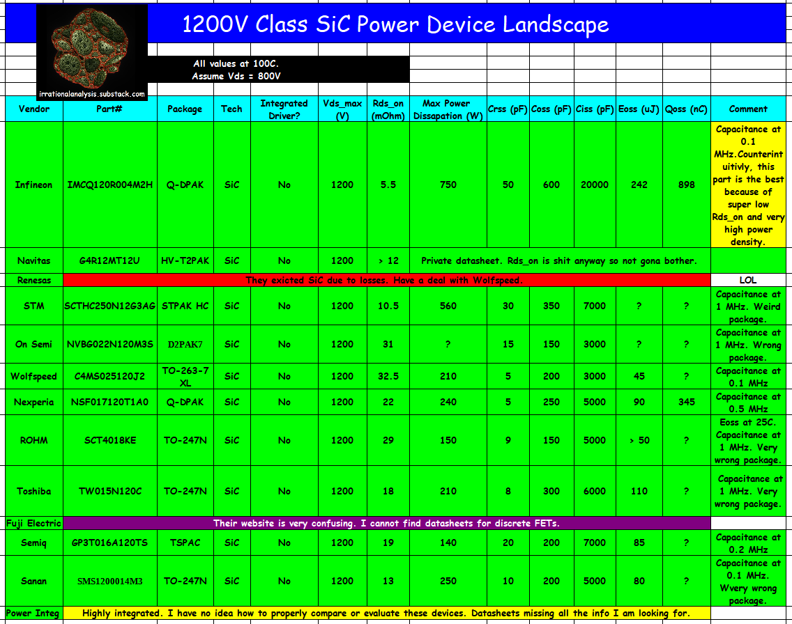
Infineon wins with extraordinarily low Rds_on. The capacitance numbers are huge but so is the density. This thing can handle insane power in a single, compact device with proper topside cooling.
I chose 100C case temperature for comparison as a conservative setpoint. With good liquid cooling, you can hit like 80C and this crazy part can dissipate 800W of power!
Who gives a fuck that your capacitance is high. Run in slow at 0.1 MHz, make inductors bigger, only use one of these instead of like 3-4 competitor parts with significantly worse Rds_on.
Infineon crushes this category.
[4.c] SiC 1700-2000V class
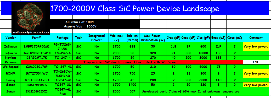
Weird category. All of the place.
Infineon win via their 2000V part (the 1700 part is dogshit), Navitas second place. Everyone else dogshit.
[4.d] Wolfspeed 10KV Madness
There are no SiC transistors in the world that can handle more than 2000V. Infineon has some modules (half bridge, two transistor) that go up to 3300V but that is not a fair comparison. Remember, one of the rules of this whole analysis is discrete FET only. No half-bridge, full-bridge, or compound multi-power-transistor devices. Only control electronics allowed as an exception.
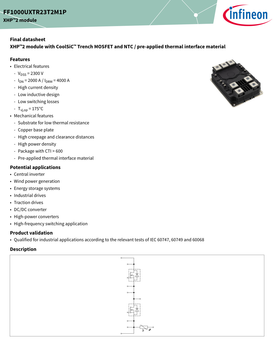
See the two power transistors? This does not count. Infineon SiC stops at 2000V under my definition.
So… let’s take a look at the Wolfspeed datasheet in detail.
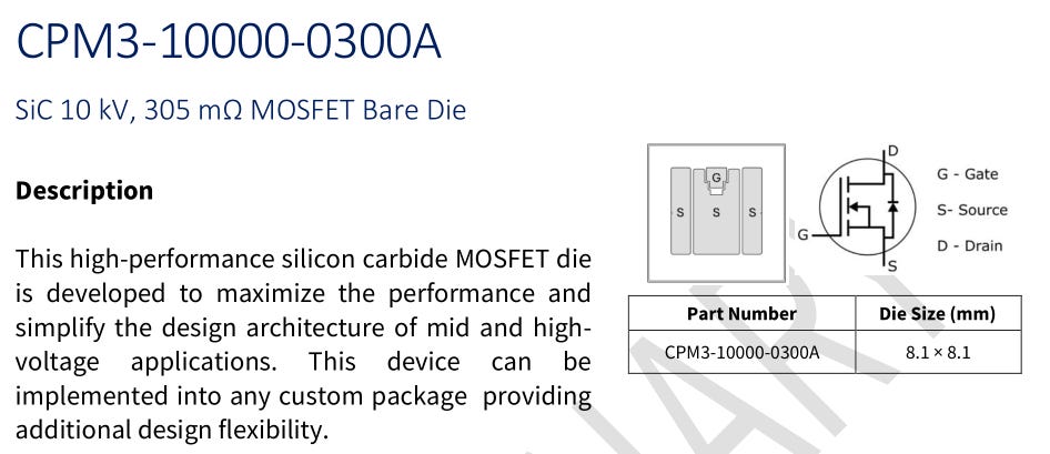
Bare die is fine given how crazy this part is.
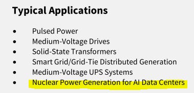
Really guys? You reaching here lol.
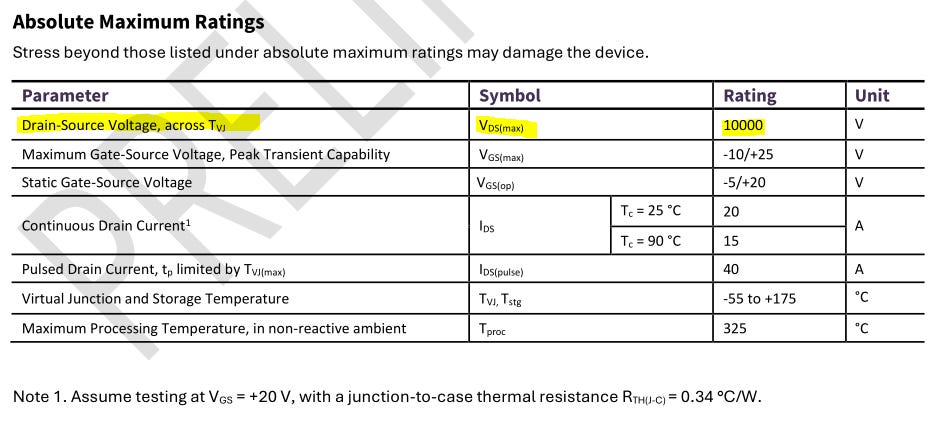
Remember you never want to be anywhere close to Vds_max. Let’s get a clue on what voltage Wolfspeed recommends for this part.
3000-6000V. Ok understandable. Still crazy.
Rds_on degrades… very severely against temperature. Even at a conservative 100C, you get 2x so 610 mOhm. Custom package and cooling needed to use this part. It’s gona kick out a comical amount of head in such a small footprint.
Parasitic capacitance is surprisingly good. I was expecting it to be much worse.
Switching losses are fairly insensitive to temperature.
Overall, I am quite bullish on the Wolfspeed 10KV part. It enables massive simplification of solid-state transformers and grid infrastructure. If and only if the customer designs package and cooling around this part.
Rds_on is super sensitive to temperature. You need good water cooling to keep this thing at good efficiency.
[5] Driver Integration, Protection Circuits, Buffers == VALUE
Let’s talk abut driver integration and protection circuits. SerDes me thinks “buffer” but perhaps this is the wrong analogy.
The main reason I rate TI and Navitas GaN above Infineon GaN is because of these integrated features. To understand why, let’s look at an Infineon application note on GaN driving recommendations!
Power semi circuit design is easy to fuck up. This is why all the companies have detailed (15+ page) application notes and teams of application engineers to support customers. Many designers choose parts based on customer support quality. In the low-voltage world, I know designers who prefer ADI/TI/MPS simply because the application engineers and support documentation are more helpful.
GaN transistors have very low threshold voltage. Too low. It creates control issues.
Negative gate drive voltage is required to proper operation. This makes the control circuits much more complicated. Really everyone, this is so fucking annoying lol.
Infineon tries to make your life easier by selling a custom GaN driver. Does the above schematic still look complicated? It is complicated!
Let’s compare Infineon’s solution with TI/Navitas.
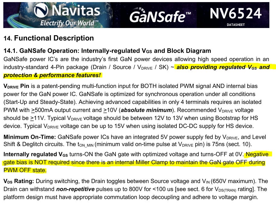
TI integrates all the painful driver shit into the same package as the GaN FET. You just use simple PWM control as if this was a normal Si or SiC part.
There is the integrated negative gate voltage circuit. All of it is done for you.
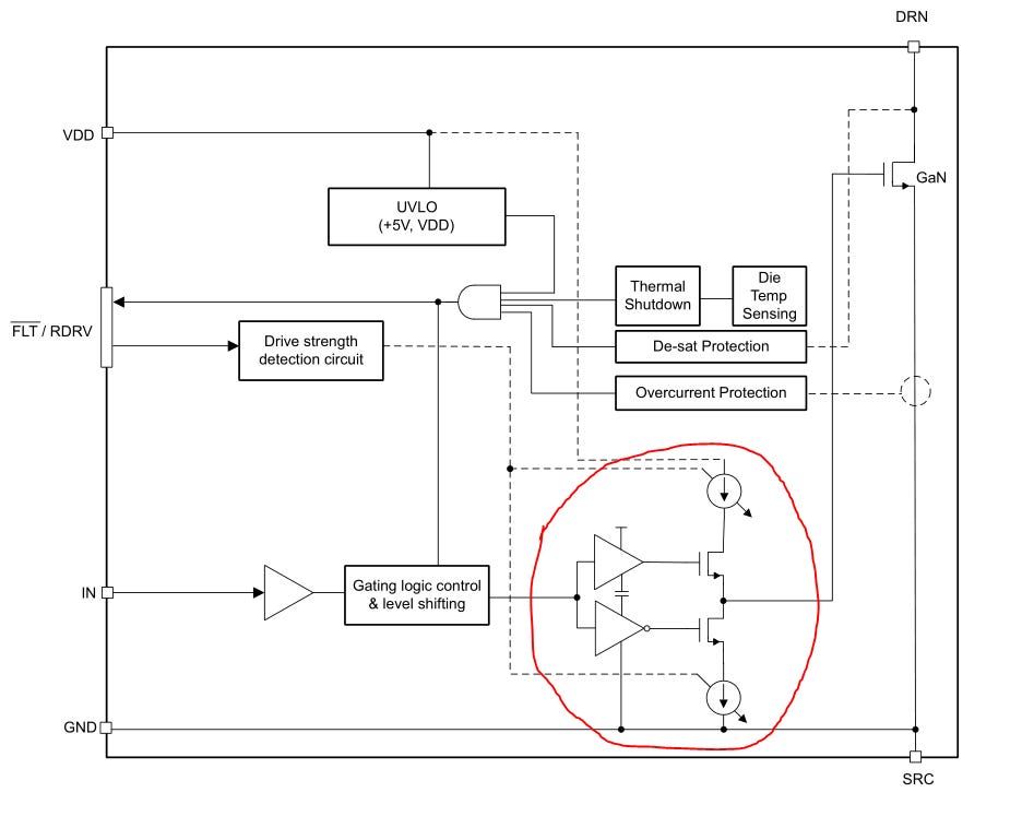
Navitas has something very similar. Arguably better as they include extra protection circuity.
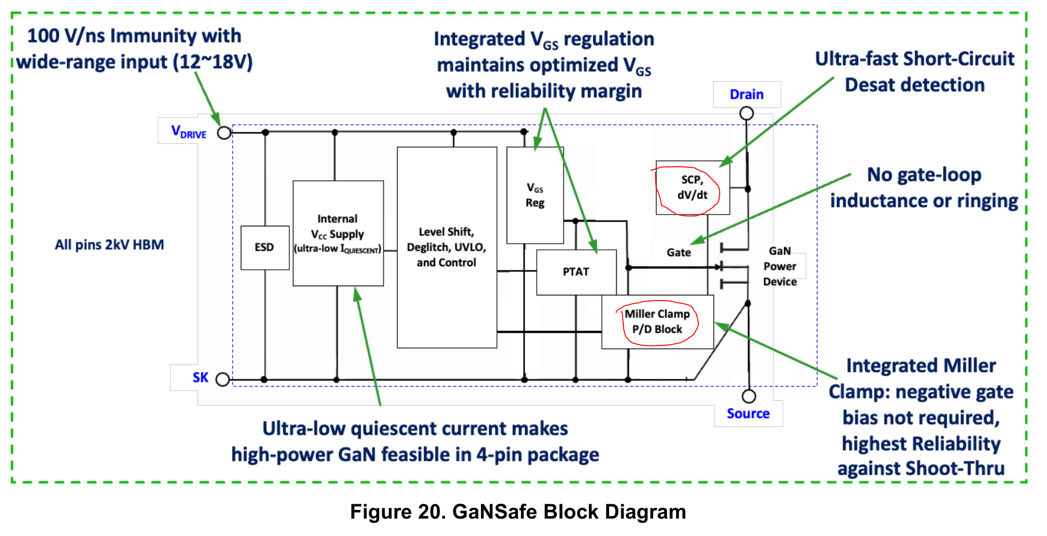
Integrated short-circuit protection is a great feature. I am not familiar with Miller clamps so let’s find out together what that is…

Ah so it’s just an extra transistor that that protects the gate driver by sending nasty pulses to ground. Seems similar in spirit to spamming Shockley diodes on all drive circuitry.
Anyway, my point here that I really realaaaallly want everyone to understand is integrated protection in GaN devices is very valuable.
Only TI and Navitas have both integrated protection and high-quality GaN FET. Nobody else has both.
[6] Multi-Sourcing, A Practical Perspective
Multi-sourcing is very common in power electronics world. Everyone has 2-3 sources for a particular product, sometimes 4. This is necessary for supply-chain reasons.
To understand what kind of work it takes to qualify a new part for an existing design, it is best to go through an example. Infineon has a nice SiC application note so I will use that.
These detailed guides and documents are public because the consequence of mistake is kaboom. You do not see this kind of stuff from TSMC floating on the free and open internet. :)
A LLC resonant converter consists of four parts:
Two strong SiC transistors.
A resonant tank consisting of one capacitor and two inductors.
A transformer+rectifier consisting of three inductors and two diodes.
At least one output filtering/decoupling capacitor.
I will skip 14 pages of math and go directly to what we chare about, how the MOSFET selection effects the design.
Remember, Rds_on is the most important parameter.
In general, lower is better so the design should be set up to support the least resistive transistor available. However, the way certain resonant designs work means you want a specific Rds_on to get optimal efficiency in some cases. This is why All the manufactures offer 5+ versions of the same transistor with varying Rds_on.
Designs also have an optimal switching speed. This is where GaN excels, offering higher switching frequencies than SiC and enabling a wider design space.
Multi-sourcing is not easy. A lot of math and simulations have to be re-done. And most importantly, markets which are sensitive to efficiency and footprint cannot second-source lower quality parts. EV you can just add bigger battery or spam more stages. You cant do this in datacenter. There is a fundamental shift coming to SiC+GaN world where quality matters again. Winners will have gross margin go up.
[7] EPIC OPPERTUNITY: Solid-State Transformers
Do you remember the Pytorch.power_plant_no_blow_up flag?

Meta (maintains the Pytorch ML framework open-source tool) added this funny flag a year ago because some grid operator got mad at them.
You see, datacenters are very unpleasant for the electrical grid. Say you have 100K GPUs training, each drawing 500W of power. During training, some large subset (say 20K GPU) drop down to 200W because they don’t need to run at full math speed for whatever reason. Waiting for all-reduce whatever.
That is a 6 MW load drop. Followed by a spike up later.
Power grids are not designed for this level of unhinged transient loads.
(its not the power plant that blows up… its the grid itself…)

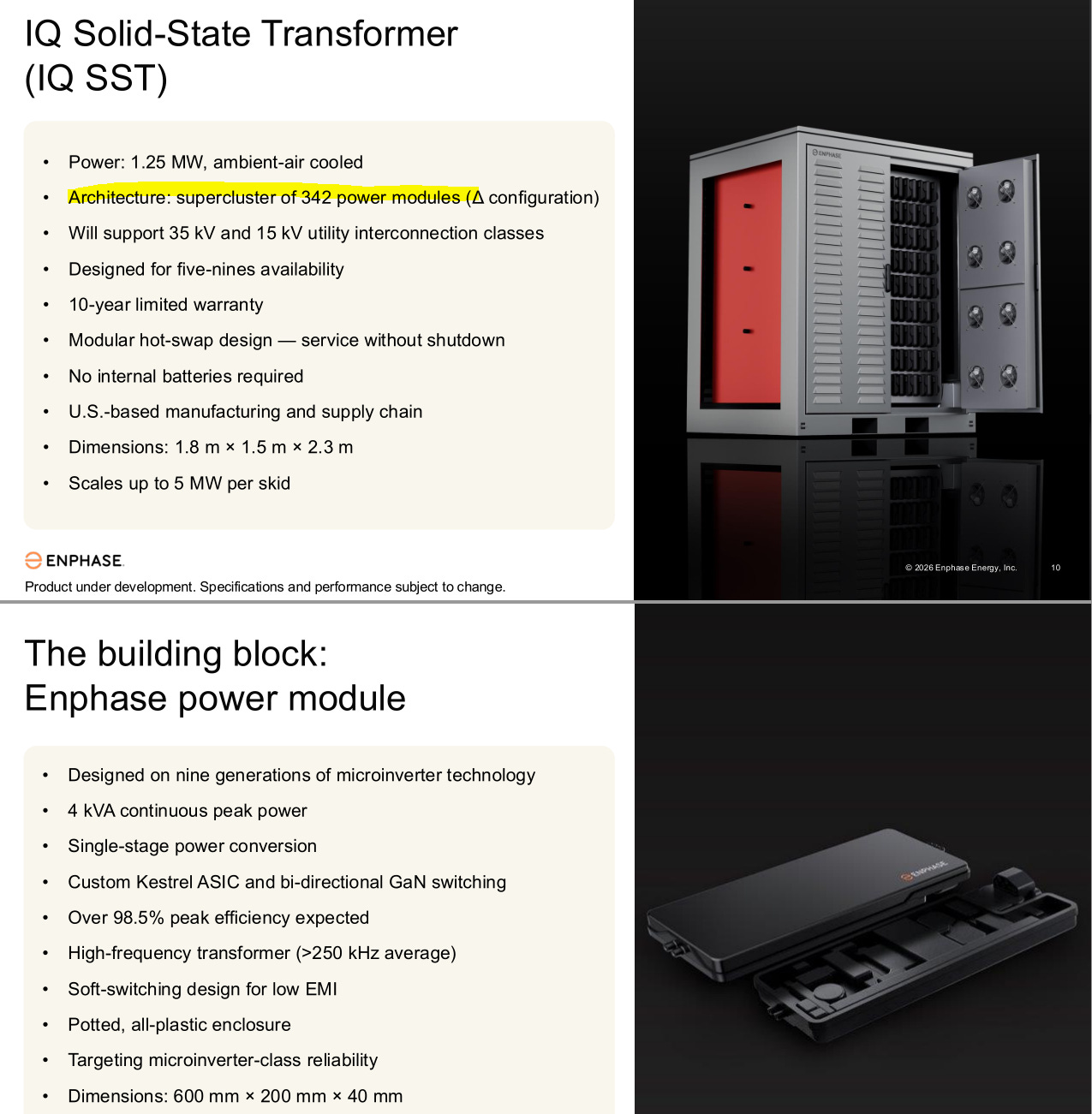
This is a high-voltage transformer. You have probably seen some of these at some point. They come in multiple sizes.

These are surprisingly simple devices. Basically giant inductors and capacitors.

What’s nice about these is they are cheap. Basically a hunk of metal with very simple construction and effectively zero moving or active parts.
Lead time is long but its so cheap nobody cares, until now.
The alternative to traditional transformers is called solid-state transformer (SST). IDK why it is called solid-state because the traditional transformers also solid state but whatever. People have talked about this SST tech for a while. Take this 4-year old YouTube video.
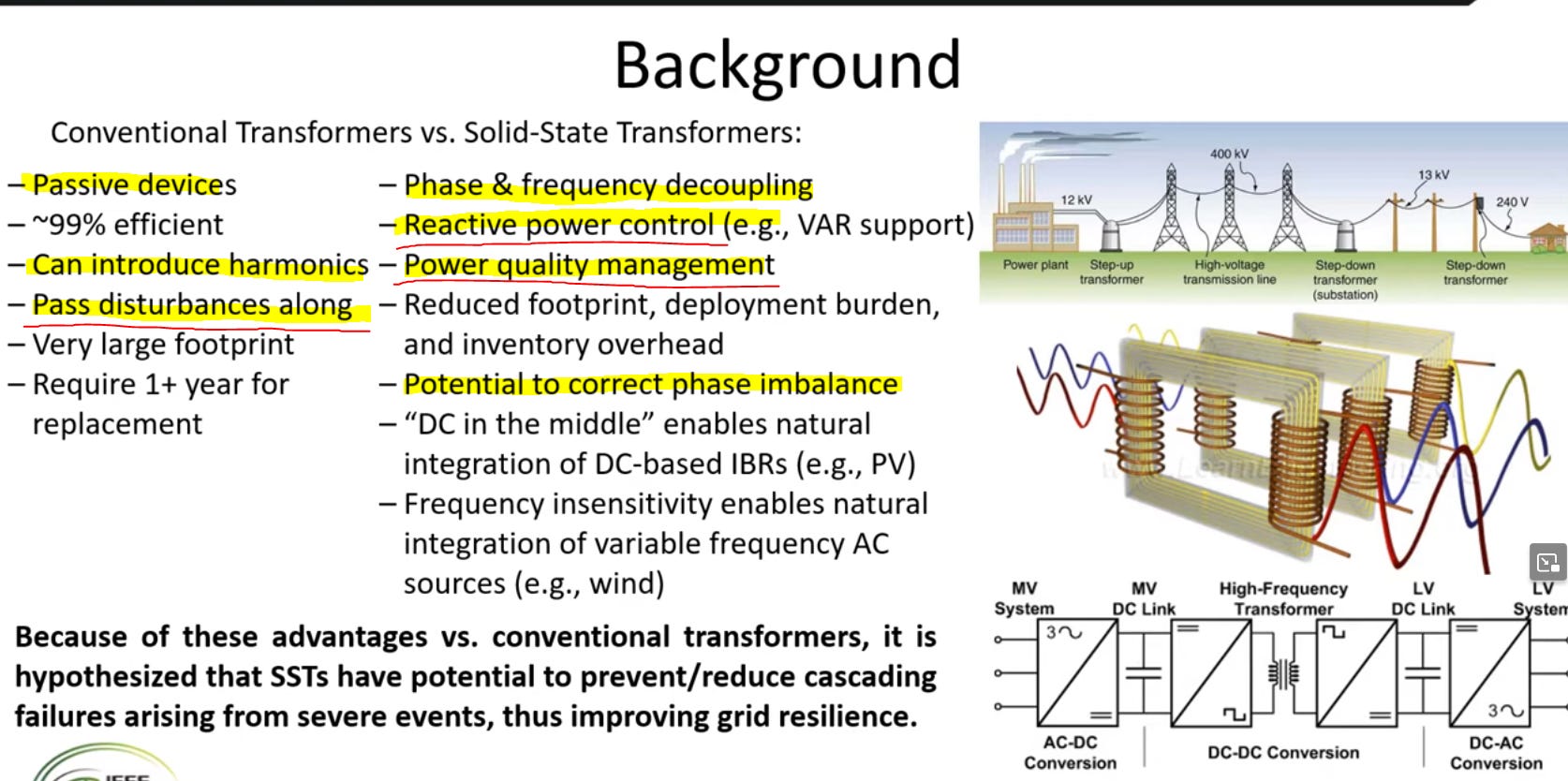
You see, when a load (AI datacenter, factory, whatever) changes rapidly, it “pulls” on the grid, creating noise and back-propagating phase/voltage/current ripple. The normal transformers just pass along whatever crap the nasty tenant creates, leading to grid instability issues.
SST never really took off because it was too expensive. Nobody wanted to pay a premium for load/voltage/current/phase regulation.
I am incredibly bullish SST. Way more bullish than the SiC/GaN companies themselves.
Do you know what reactive power is?
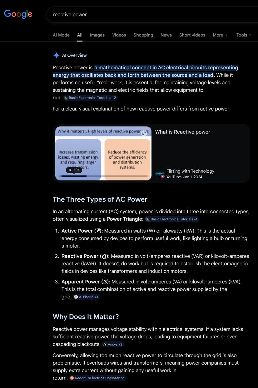
If you have 1GW of electrical generation and 1GW of load, you are fucked. It’s not just transmission losses that lead to a gap between supply and demand, a non-trivial amount of power (reactive power) is needed to “push” the electricity through the grid and various types of loads.
All those AI datacenters having trouble getting permits and grid connections… you know why? Because the power grid operating knows that shit is gona take everything down.
It’s not just the amount of power being asked, its the type of load. Dynamic (destabilizing) load that guzzles reactive power too!
Solid-State Transformers not only help with load regulation (you don’t have to stupidly keep all GPU/ASIC at full power), it also helps reduce reactive power needs!
You are not bullish enough on SST. Unironically I believe SST opportunity is much larger and more attractive (from margin perspective) than inside datacenter power. Everyone is focused on the wrong thing. The power chips going between grid and datacenter are the real opportunity, not the Nvidia or OCP power rack.
TRADITIONAL TRANSFORMERS ARE THE ELECTRICAL-ENGINEERING EQUIVILANT OF A STONE WHEEL. ITS TIME TO UPGRADE. AI DATACENTERS ARE A MUCH STRONGER CATALIST THAN PEOPLE THINK. THE PREMIUM PRICE IS TOTALLY JUSTIFIED.
[8] Public Market Investment Corner
First, disclosures.
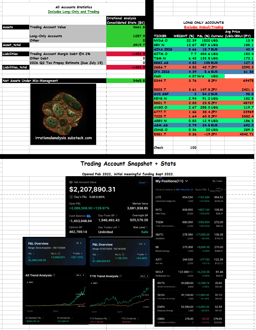
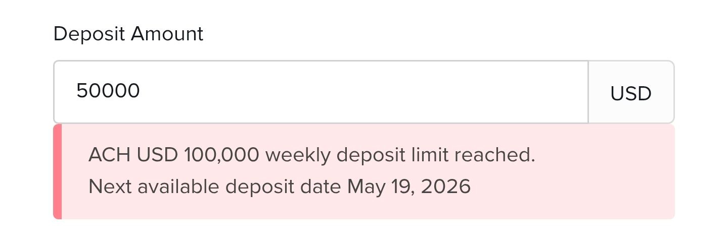
I have 50K waiting to go into IFX but Interactive Brokers has some stupid limit on deposits.
That 50K is going into more IFX and AIXA. Have not decided on the split yet.
I strongly believe that exposure to both GaN and SiC is desirable.
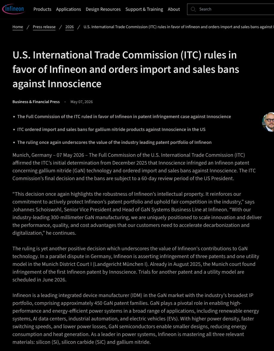
For GaN, TI and Navitas have the best parts while Infineon in second place. TI is not a pure-play so I sold out. FYI Infineon has a very recent patent case against Innoscience. Navitas and Infineon also have a cross-licensing and second-sourcing agreement.
A hedge fund friend tells me that On Semi and STM both buy GaN wafers from Innoscience which will… have problems going forward. IFX makes their own GaN wafers and Navitas is fabless using GloFo wafers. Bullish IFX and GFS. GloFo losers are not getting any meaningful SiPho volume so at least they can use cleanroom space for lower margin GaN.
On Semi has exciting vertical GaN technology but there are no public datasheets. This is just a bunch of hopes and dreams on slides. I sold out at nice 15% profit in like 2 weeks because after completing full DD, their SiC is meh and lateral GaN meh. If anyone has real technical info on ON 0.00%↑ vertical GaN, email me.
Infineon has a dominant position in SiC. Crush everyone in 1200V category. For 1700-2000V, Navitas is ok (Infineon still beats them) and everyone else is shit.
I believe the Wolfspeed 10KV part will play a huge roll in SST revolution. Enables drastic reduction in control complexity.
For semicap, I am now even more bullish Aixtron. Was buying for InP but they also have almost monopoly position in GaN. This is a STONK.
Finally, some wildcard picks. The companies that actually make SST are Delta Electronics and other large well-diversified, respected firms. The Vertivs and Eatons of the world.
If you want safe outperformance, go for Delta Electronics.
If you want degen shit to gamble… let me introduce you to ENPH 0.00%↑ and SEDG 0.00%↑, two corpses.
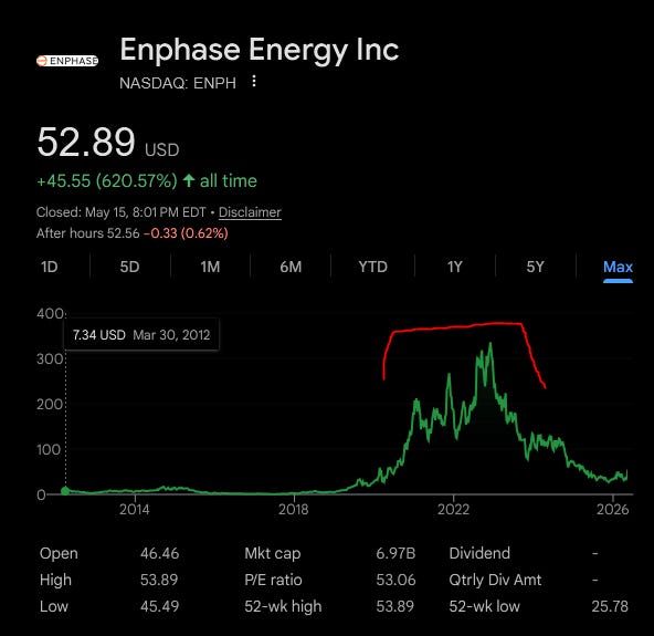
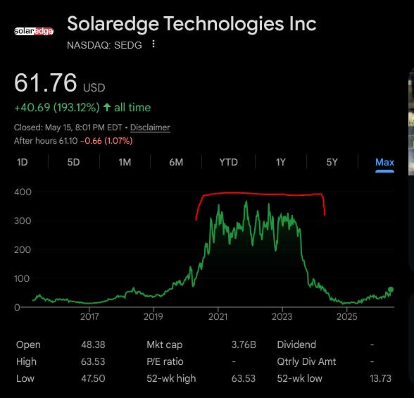
Both of these shitcos are in the home solar market, which is fucking dead now that tax credits are gone.
You see, solar panels are high-voltage DC but your house is low-voltage AC. So each solar panel needs a DC to AC inverter and all of these “micro-inverters” need to be controlled in a safe way such that they are in the correct phase and can interface both to your house and the grid.


This is a distributed systems problem where safety is critical. The consequence of failure includes but is not limited to:
Dead technition
Fire
Dead/crispy customers after house burns down
Grid damage and lawsuit from grid operator
The real value-add of these companies is not the power circuit design itself. It is all the safety circuits and control circuits.
Remember the examples section…?
It takes only four fucking transistors to convert 500V DC to 200V AC. The hard part is making this circuit safe, linking many copies together, and controlling it all.
Enphase and Solaredge core competence is this shit. Several hedge funds have expressed doubt and I am like guys wait for the post. You will see circuit diagrams and understand what I am saying. Hey Clark, did you convince your smooth-brain boss to download LTSpice?
Placing a bunch of these things in one environmentally protected box is easier than spreading them out over a roof that is exposed to the elements.
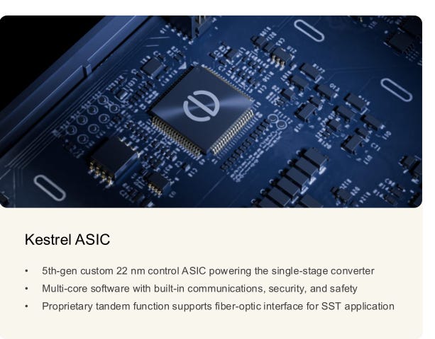
They have a fucking 22nm logic ASIC for control! You know all those STM microcontrollers are in shortage because of optical transceiver ramp right?
Some behind-the-scenes. For weeks people have been pinging me on this crap. 18 months ago I DD both of them for unrelated reasons and determined its dogshit. After the 15th fucking person sends me these two shitcos, I finally spend some time and… its not stupid. Its hilarious.

My entire job for the last decade was to create those spice model files for transistors that you put up a screen shot of. It's a degenerate job of editing text files for a living, and dealing with simulators with terrible documentation. Thank god for Substack.
I am not smart enough to comment on power semis, so here is Claude 😂:
Good read — I've got the full article. Given your deep semiconductor knowledge, I'll give you a thorough breakdown. Overall it's **largely technically sound**, but there are a few places worth scrutinising.
---
## ✅ What's Correct
**SiC vs GaN tradeoffs**
The core framing is accurate. GaN enables higher switching frequencies at lower voltages; SiC handles higher voltages and power density. This is well-established physics. The article correctly notes GaN is currently limited to ~650V class for lateral devices while SiC extends to 1200V, 1700V, and beyond.
**Rds_on as the key figure of merit**
Correct — this is the dominant driver of conduction losses. The article's emphasis on it over headline Vds ratings is the right engineering instinct.
**Gate charge and parasitic capacitance**
The explanations of Qg, Qoss, and Eoss are technically accurate and correctly linked to switching losses and efficiency.
**Negative gate drive requirement for GaN**
Accurate. Lateral GaN HEMTs (depletion-mode devices) have very low threshold voltages and can suffer spurious turn-on without a negative gate bias during off-state. This is a genuine design pain point that TI and Navitas address through integration.
**TI and Navitas GaN integration advantage**
Correct that integrating the gate driver, negative bias generation, and protection circuits into the same package significantly reduces design complexity. This is the "GaNFast" approach Navitas pioneered and TI has followed. It's a real differentiation.
**Infineon's SiC strength at 1200V**
Generally well-supported. Infineon's CoolSiC MOSFET technology is widely regarded as among the best-in-class, particularly in 1200V. Their trench-based SiC MOSFETs have industry-leading Rds_on per unit area.
**Wolfspeed 10kV SiC**
The device exists and the characterisation of it as niche but potentially transformative is fair. The Rds_on sensitivity to temperature is a real challenge, and the article correctly flags that custom packaging and cooling are necessary.
**Solid-State Transformers (SST) and reactive power**
The underlying concepts are correct. SSTs do offer active power factor correction, load buffering, and reactive power management that passive transformers cannot. The argument that AI datacenters create destabilising transient loads is valid — the PyTorch flag reference is real and well-known in the industry.
**Multi-sourcing complexity**
The point that qualifying a new transistor in an existing design is non-trivial (especially for efficiency-sensitive applications like datacenters) is accurate and often underappreciated.
**Aixtron MOCVD near-monopoly for GaN**
Correct. Aixtron dominates GaN epitaxy tool supply (MOCVD reactors), which is a genuine bottleneck. This is a legitimate semicap angle.
---
## ⚠️ What's Questionable or Needs Nuance
**"GaN is limited to 650V only"**
This is partially outdated. Vertical GaN is actively being developed by multiple players (including ON Semi, Transphorm, and others) and is designed to breach the 650V ceiling. The article itself acknowledges ON Semi's vertical GaN but dismisses it as "hopes and dreams on slides." That may be too harsh — Transphorm, for instance, has been selling vertical-architecture GaN at 650V and is working on 900V+ devices. The ceiling is more like a current commercial limit than a hard physical one.
**Navitas SiC being "shit"**
Directionally fair for now, but Navitas acquired GeneSiC in 2022 specifically to build a credible SiC portfolio. GeneSiC had strong technology, particularly for higher-voltage SiC. Calling Navitas SiC categorically poor without engaging with the GeneSiC heritage is a bit superficial.
**"Nobody cares if both GaN and SiC come from the same company"**
This is probably true at the discrete transistor design level, but less true at the system/module level where vendors selling complete reference designs and power modules benefit from offering a unified portfolio with validated cross-family designs. It's not purely a silly marketing claim.
**Infineon patent case against Innoscience**
Mentioned briefly and presented as straightforwardly bullish for Infineon/GloFo. The reality is patent disputes in semiconductors take years and outcomes are uncertain. Innoscience is also a large, well-capitalised Chinese IDM — treating the patent case as a settled negative for them is premature.
**STM buying GaN wafers from Innoscience**
Plausible and has been reported in trade press, but the article presents this as confirmed fact. STM has its own GaN-on-Si development as well. The supply relationship may be partial or transitional rather than a total dependency.
**"Traditional transformers are basically inductors and capacitors"**
A slight oversimplification for the purposes of this article. Traditional power transformers are magnetically coupled inductors — there are no capacitors in the core design. The article may conflate the power transformer with the broader substation equipment (including capacitor banks for power factor correction). Minor but worth noting.
**SST "never took off because it was too expensive"**
True but incomplete. SSTs also face reliability and maturity concerns compared to passive transformers that have a 100-year reliability track record. Utilities are conservative buyers. The cost barrier is real but it's not the only barrier.
---
## Summary Verdict
| Area | Assessment |
|---|---|
| SiC/GaN physics | ✅ Solid |
| Datasheet analysis methodology | ✅ Sound |
| Infineon SiC leadership | ✅ Accurate |
| TI/Navitas GaN integration | ✅ Accurate |
| GaN 650V ceiling | ⚠️ Oversimplified |
| Navitas SiC dismissal | ⚠️ Too harsh (ignores GeneSiC) |
| SST opportunity thesis | ✅ Directionally compelling, some nuance missing |
| Aixtron/GloFo angle | ✅ Legitimate |
| Innoscience patent/supply claims | ⚠️ Stated with more certainty than warranted |
The author clearly has genuine technical depth — the datasheet walkthrough and circuit intuition sections are better than most sell-side content on this topic. The investment framing is reasonable but benefits from the bullishness being occasionally stronger than the evidence strictly supports.